This thread has been locked.

If you have a related question, please click the "Ask a related question" button in the top right corner. The newly created question will be automatically linked to this question.

ISO5852S: Soft Turn OFF

Part Number: ISO5852S

Hi,

I am using ISO5852S for a IGBT Short circuit test. A DC Link voltage of 350-500V is given directly across one IGBT and made that IGBT ON. I have found even though primary side fault signal is made low. The gate emitter voltage doesn't reduce and hence the soft turn off doesnt happen. After Fault detection I had observed a DC link raise is occuring. What may be possible causes for Soft turn off not to happen ??? 

  • Hi Manoj,

    Can you please share your test circuit and waveform captures?

    Also, I think that your SC testing method is less conventional than I have typically seen. More commonly, the DUT is tested in a half-bridge with an inductive load to generate the SC current under various conditions. A good application note discussing SC test methods is given in this application note.

    Regards,

    Audrey

  • Dear Sir,

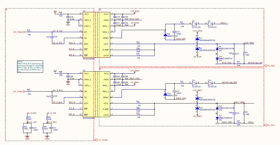
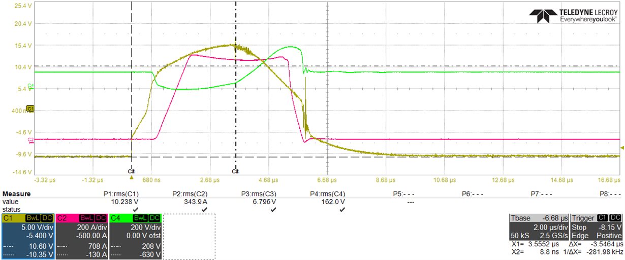
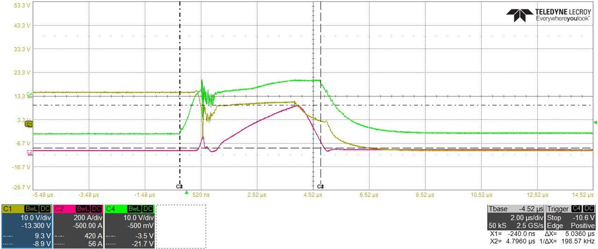
    Thanks for sharing the document. We have not measured the inductance value. Also we have conducted the test as per SC Mode 1, where a small wire is connected across one IGBT. And the other IGBT we had given a high pulse. Please find the attached ISO5852S test circuits and the waveforms captured.

    CH1 DC Link Voltage ,  CH2 Device Current ,  CH3 Fault signal from Driver, CH4 Gate Emitter Voltage. 

    Even after Fault receive the gate emitter voltage is not reducing, I hope it may due to miller effect. Hence unable to see the soft turn on feature and current clamping down immediately.

  • Hi Manoj,

    Thanks for sharing the circuit information and waveforms.

    When the VGE does return low at around 5.8us, is this due to the input signal or is it due to DESAT detection?

    Can you also include the waveform of the DESAT pin to GND2?

    Regards,

    Audrey

  • Dear Sir,

    It is due to input signal. We didnt capture DESAT voltage waveform. 

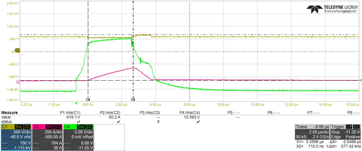
    However with ISO5852S-Q1 things are working fine.. We have tried two-three nos of different ICs of ISO5852S. The waveforms was similiar. 

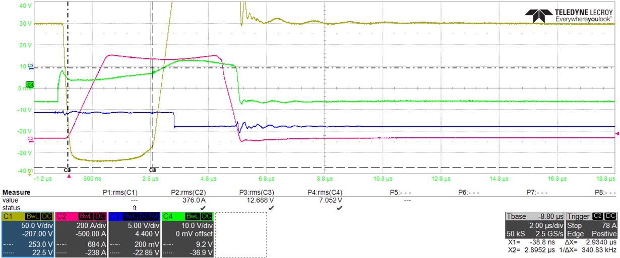
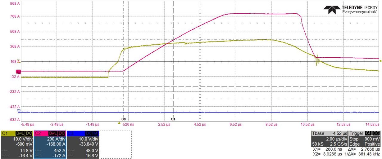
    Waveforms with ISO5852S-Q1 are included below for reference. What may be the reason not to work with ISO5852-S ?? 

    CH1- DC Link Voltage, CH2-  Current , CH3- Gate Emitter Voltage, CH4- DESAT pin w.r.t GND2

    Regards

    Manoj.R

  • Hi Manoj,

    The ISO5852S and ISO5852S-Q1 functionality should be the same. It seems to be a system difference which may cause the change in the DESAT performance. Is the test setup and board the same between the two tests you have shown? Are you swapping the part on the same board without changing anything else?

    Regards,

    Audrey

  • Dear Sir,

    The test set up and board is same. Part is also not swapped. WIth ISO5852S we found DESAT w.r.t GND Desat Diodes in floating mode without connecting to collector point. It is able to block by 3us and soft turn off also happens,waveform is sawtooth. But with Desat diodes connected to Collector. The Desat w.r.t GND is getting disturbed.

    Whereas with ISO5852S-Q1 we are getting the results as intended.

    Regards

    Manoj.R

  • Hi Manoj,

    When you say that the DESAT w.r.t. GND is getting disturbed, do you mean that it no longer is initiating STO + fault signal? Can you also try measuring directly at OUTL to see if driver is pulling down?

    Also from the above screenshots from the oscilloscope, it seems the two test conditions are different. The short circuit current in the first scenario looks much higher than in the second case.

    I would also ask that you swap out the ISO5852S-Q1 with the ISO5852S on the good test board to ensure there is nothing different between the two boards. It would also be beneficial to replace the ISO5852S with another ISO5852S to see if you still have the same problem. Have you done this?

    Regards,

    Audrey

  • Dear Sir,

    I am sorry we were held up with some other activities. Our application needs to go with ISO5852S-Q1 hence we have proceeded with the same.

    We are currently facing one issue. We are currently using ISO5852S-Q1.

    Case 1:

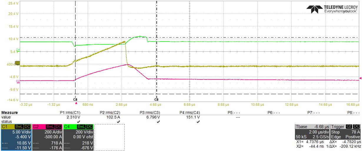
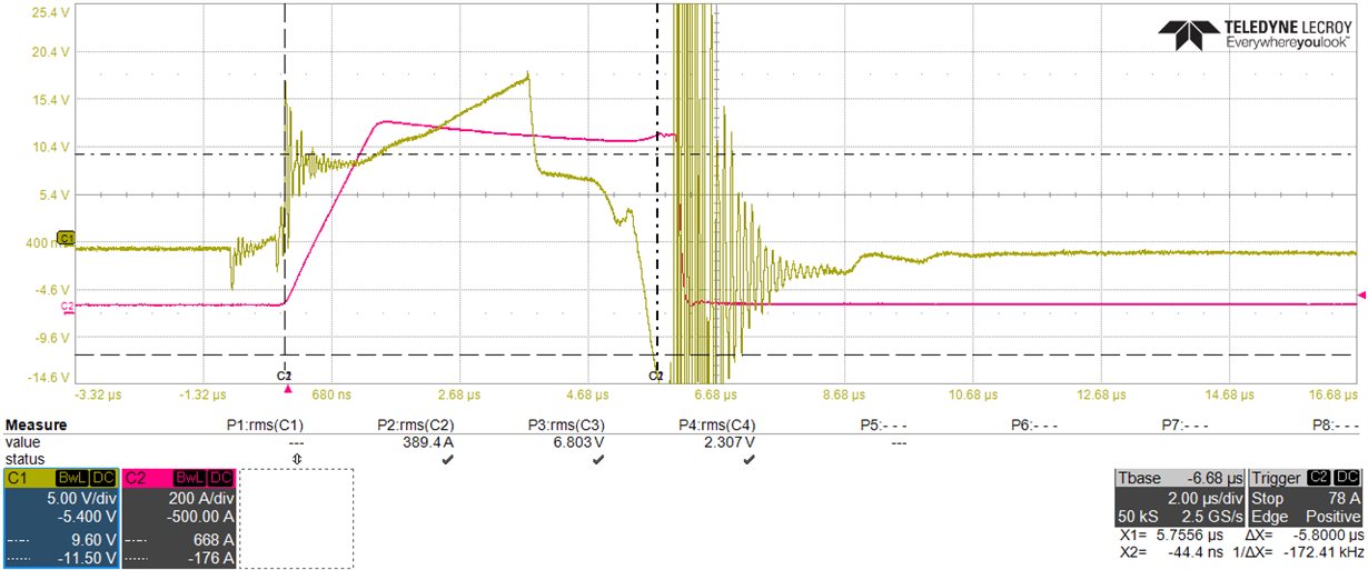
    Bottom IGBT SC. In this case Vdc(+) to Rphase an external wire is connected. And a 5us pulse is given to bottom IGBT. Channel 1 DESAT w.r.t GND. CH2 : DC Link Current  Figure 1. The fault is been detected within 3.5us. 

    Case 2:

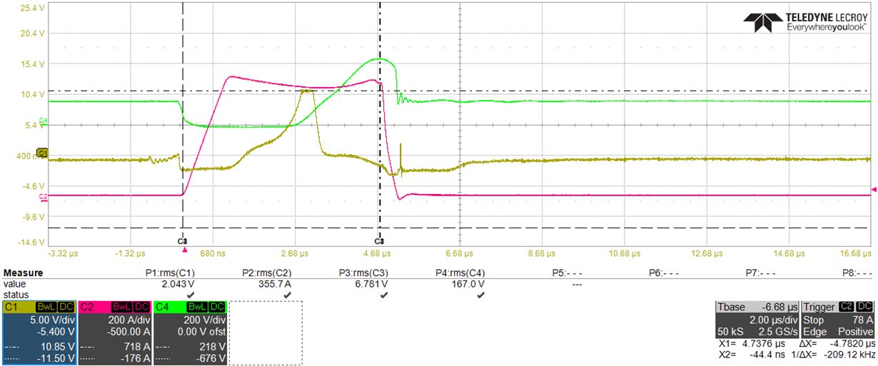
    Top IGBT SC. In this case Rphase to VDC(-) we have connected through a external wire. And a 5us pulse is given to top IGBT. Channel 1 DESAT w.r.t GND. CH2 : DC Link Current. Figure 2.

    We are observing with all the top and bottom gate drivers the same behavior.

    What may be the reason for DESAT voltage is getting distorted in case of TOP gate Drivers?? And current is higher??  Please help us on the same. Looking forward for your support. 

  • Dear Sir, 

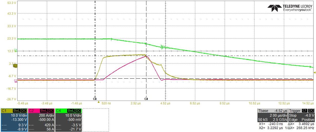
    Please find the Gate Emitter Voltage also for reference.

    CH1: DC Link Voltage , CH2 : SC Current CH4: Gate Emitter Voltage withTop driver. 

    CH1: DC Link Voltage , CH2 : SC Current CH4: Gate Emitter Voltage with Bottom driver.

  • Hello Manoj,

    The di/dt may be faster for the HS device due to the lower loop inductance (when the LS device is tested, there is additional inductance due to the wire shorting the HS device). It looks to be the case when VDC is around 200V in the example you show. The faster transient can also result in a more distorted voltage waveform on the DESAT pin. However, it looks like DESAT is still detected and STO has been initiated, although at a higher SC current so the turn off transient is longer. Do you use the same gate resistance for both the HS and LS?

    Additionally, it may be useful to see if there is a change in your measurement if you measure the HS DESAT pin w.r.t Phase node instead of GND in case of inductance between the Phase node and GND.

    Regards,

    Audrey

  • Dear Sir,

    We are using the same gate resistance for TOP and Bottom Device. Please note that we are using the same wire for shorting. While top gate driver is tested the bottom device is externally connected through a wire R Phase to VDC(-). The same is only used while testing the bottom device, shorting Vdc(+) to R Phase.

    However the PWM routing length's are different in the PCB layout. Please find the attached DEsat Pin w.r.t to device GND.(R Phase) . 

    What may be the probable causes for distortion of DESAT waveforms.?? Is there any chance of layout related issues. ??

  • Hi Manoj,

    It looks to be that the di/dt is faster for the HS because the drain inductance is much smaller. This could result in more noise on the DESAT pin. The di/dt is lower for the LS because of the added inductance from the wire you use to short the HS.

    Please try to do the SC test in the following way:
    When testing the LS as DUT:
    - Hold the HS on with 15V then apply short pulse to the LS (better to use higher VGE>15V if possible so that the LS saturates first).
    When testing the HS as DUT:
    - Hold the LS on with 15V and apply a short pulse to the HS (better to use higher VGE if possible so that the HS saturates first).

    Please try the SC test method I mentioned above and let me know if you see a change.

    The last waveform you sent looks like noise due to the measurement. What kind of probes are you using? Are the probes nearby one another? There could also be noise coupling between them.

    With respect to layout, the DESAT capacitor should be close to the DESAT pin to help with noisy signals.

    Regards,
    Audrey

  • Dear SIr,

    If HS is given +15V the HS device will be already ON. I didnt understand how the LS device saturates first if I am giving short pulse further to LS.

    We are using active probe and not so closer too.When the device undergo SC even we have observed the noise in the input side.

    We have placed DESAT cap near to DESAT pin only with all gate drivers. However the PWM routing lengths are different. DC(+) layout is different from VDC(-)

    Regards

    Manoj.R

  • Dear Sir,

    Please find the observations below,

    The time duration of Pulse is 5us.

    Case 1: When TOP is ON and Bottom is given Pulse , before the fault detection the GATE Emitter Voltage of HS  is going down. 

    Case 2: When BOTTOM is ON and TOP is given 5us pulse, the LS device detects the fault .

    Also it is observed that at lower voltages DC Link Voltage <100 V while shorting the TOP device even though the input pulse duration is 5us, the GATE Emitter Voltage exists for more time.  What may be the probable reason?? This is the same case with all gate drivers.

    At higher voltages the fault detection is at lesser time , however device goes to saturation and current is  more. While repeating the SC current many times there are device failures too. Please convey us what we can conclude from these experiments. 

  • Hi Manoj,

    I have a correction to the previous statement: the pulsed DUT should have smaller VGE. This is because the HS is held on with higher VGE, and thus has higher saturation current. The LS VGE (being smaller) has a lower saturation current, and will saturate faster to protect first.

    This is as shown in the figure below. VGE1 is the device held ON and VGE2 is the pulsed DUT. The chosen VGE should be within the limits as given in the IGBT datasheet.

    The di/dt is a function of Vdc and the parasitic inductance. With smaller Vdc, there is slower di/dt. In the case where Vdc<100V, the short circuit current takes longer time to ramp up.

    With higher Vdc, the short circuit current will ramp up much faster, higher di/dt. This will cause the IGBT to saturate faster.

    Please make the above recommended change to your test. The test should now properly show the DESAT protection for the driver IC.

    Regards,

    Audrey