This thread has been locked.

If you have a related question, please click the "Ask a related question" button in the top right corner. The newly created question will be automatically linked to this question.

Current draw problem with TPS40200

Other Parts Discussed in Thread: TPS40200

I am having a problem with a circuit that uses the TPS40200. I used SwitcherPro to design a 9V power supply with the following inputs:

Vin Min = 12V

Vin Max = 50V

Vout = 9V

Iout Max = 2.9A

SwitcherPro gave me the following circuit, which I duplicated into my schematic:


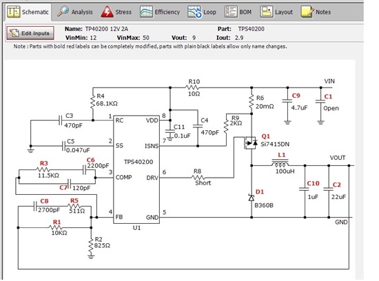
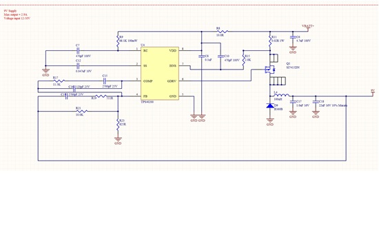
I am using the TPS40200 to step down a battery voltage of approximately 24V down to 9V, which then goes into a series of cascaded power supplies of 5V, 3.3V, and 1.8V. The load on the 9V supply draws 0.05A. The reason Iout Max = 2.9A is because our power system is designed to supply auxiliary power to external user-supplied devices which are of an unknown resistive load.

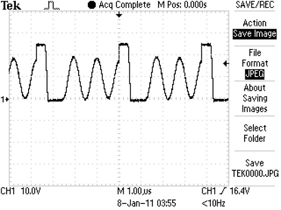
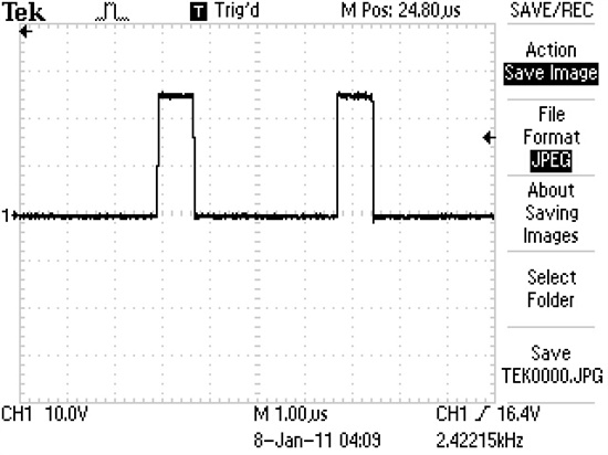
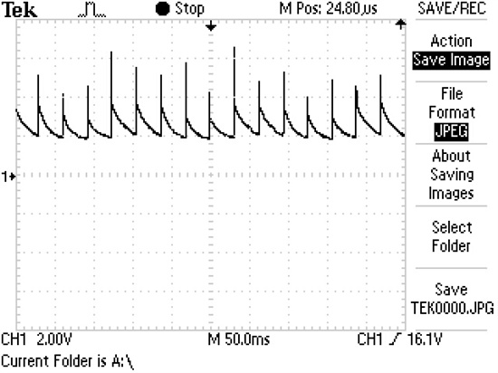
The problem I am experiencing is that this 9V power supply draws 0.2A at 24V, even when I have disconnected the output of the 9V supply to the cascaded power supplies and their loads. This is a much higher current draw than I expected. I measure 0V at the output. The cascaded power supplies below the 9V supply all work when powered from an external supply, so I am led to believe that it is a problem with the TPS40200 circuit.

When I measure the resistance between Vin (24V) and GND, I get approximately 150K. Is this value expected? I am concerned that I have a short somewhere. I have attempted to remove components to determine the source of the short, but so far, only the removal of the TPS40200 itself changes the resistance between Vin and GND.

Is there a minimum current draw requirement for this circuit to function? The datasheet does not indicate a minimum, but SwitcherPro says that Iout Max ranges from 0.1A to 3A.

Any help would be greatly appreciated. Thank you very much in advance.

Sincerely,

-Kim

  • Kimberly,

    Some small input current is expected from a converter running at no load, however 200mA does seem excessive.  I would recommend checking the 9V output to make sure it's stable and checking the components connected to the output to make sure there's no leakage path somewhere.

    If you are measuring 150kOhms VIN to GND, you don't have a short.  That's is a mear 160uA of current @ 24V and likely a measurement of the 68kOhm timing resitor (VIN to GND) and the internal protection components which can leak a small amount of current from RC to GND when the IC is unpowered.

  • I am pretty sure there is no leakage path on the 9V end. I verified this by disconnecting L1, disconnecting Vin, and applying power at the Vout point with an external 9V power supply. All the components connected to 9V functioned as expected.

    When I reconnect Vin and L1, however, the circuit draws Vin at 0.2A and Vout is 0V, instead of 9V. Q1 does not appear to be switching on, and yet something in the circuit is sinking 0.2A from the supply at Vin.

  • Kimberly,


    Can you please provide a few waveforms so we can try to figure out what the problem is?

    First, measure the drop across the 10W resistor (R10) between VIN and VDD.  This will indicate which side of this resistor the current sink is on.  I doubt the 200mA is passing through this resistor, but we should be sure.

    Next, let's look at:

    The voltage at RC at about 1V / division vertical and 5us / division horizontal scale?

    The voltage at the P-Channel GATE at 5V / division vertical scale and 5us / division horizontal scale?

    The ouptut voltage at 2V / division vertical scale and both 5us / division and 100us / division horizontal scales?


    Also, after the power supply has been running for 30-60 seconds, lightly feel around the devices.  Any components dissipating 4.8W of power (200mA x 24V) will get VERY hot.   While the hot component might not be the cause of the power dissipation, it will indicate where to look for the cause.

  • The voltage across R10 is 1.62V. The power supply shows 0.16A at 24V. That means that 0.16A is, in fact, all going through R10.

    The voltage at RC is a flat 10.4V DC, at 5us/div

    The gate voltage is 24V DC at 5us/div. It does not switch.

    The output voltage is 0V (since the gate is not switching on and off)

    If I could detect any part of the circuit that was switching or produced a waveform that wasn't DC, I could have a better idea of what was malfunctioning, but it looks as though the TPS40200 itself is simply not working. I suspected the VDD pin on the TPS40200 was sinking all the current, and when I lift pin 8 off the pad, the short disappears. I used the freeze spray method to detect thermal signs of power dissipation and the TPS40200 chip and R10 are the only components to get hot.

  • The TPS40200 may be damaged, but I'd like to check a couple of things first.


    1) Are you doing anything to hold the SS voltage low during this test?

    2) Can you check the resistance of R4?  - The voltages you reported are consistant with this being a 68.1 Ohm resistor instead of a 68.1kOhm resistor.

    If those two things check out and they're OK, it's most likely that the TPS40200 you have was damaged somehow and should be replaced.

  • Peter,

    You were right about R4. There was a mistake in the assembly process, and it was, in fact, a 68.1 ohm resistor.

    I changed it to the proper value, and I now am able to get 9V DC on the output under unloaded conditions.

    When I look at the waveform at the gate of Q1, I get a clean looking square wave. When I measure the waveform at the drain of Q1, I get the image below:

    It looks as though a sine wave is superimposed on a square wave, which I did not expect. However, the 9V output is stable when it is not loaded. When I apply a 10K resistive load to the output, it is also stable. However, when I apply the intended load (the cascaded switching regulators) to the 9V output, the voltage drops to an unsteady 3.3V DC on the output, and the waveform I measure at the drain of Q1 is:


    Now, it looks just like the square waveform in the image above, without the sine wave superimposed. The waveform at the gate is a steady 24V DC. There is no switching going on.

    When I disconnect the 9V power supply from the intended load (the cascaded power supplies) and power them from an external 9V supply, the intended load functions properly. There are no shorts in the intended load. I believe there is still something that is not functioning properly with the 9V supply. Could it be a time constant mismatch between C11/R10 and C4/R9?

    Thanks for all of your help so far!

  • To further add to the images, when I zoom out to 50ms/div, this is the waveform of the unsteady 3.3V on the output side of the 9V supply when I hook it to the intended load:

    This noise is not present in the unloaded or 10K-loaded state. There is no noise like this on the intended load side when I hook up an external 9V supply either, so I believe the problem can be attributed to the 9V circuit.

  • Kimberly,


    What you're seeing here is the TPS40200's current limit response.  When the TPS40200 controller detects a current limit event, the converter is disabled, the soft-start capacitor is discharged slowly to 150mV, then the converter is enabled and the soft-start capacitor is charged through a new soft-start cycle.

    When the converter restarts and the ouptut votlage increases again, it triggers over current and shuts down once more.

    What is most likely happening is the LDOs of the intended load are likely all turning on about the same time and drawing a large amount of current from the 9V rail together, and this spike in load current is triggering OCP, forcing the converter to shut-down and restart.


    Solutions we can look into?

    1) OCP trigger is error due to mismatch between VDD time-constant and ILIM time constant.  Here the solution would be to match these time constants and improve current limit accuracy.

    2) OCP trigger is correct and LDOs are drawing excessive current during start-up:

      2a) If the LDOs have programmable Soft-start values, increase the soft-start time of the LDOs to reduring their start-up current draw

     2b) If the LDOs have programmable UVLO, seperate their UVLO voltages so they start-up seperately

     2c) If the LDOs have enables can we sequence them to spread-out their start-up currents?

     2d) If we can't reduce the start-up currents of the LDOs or sequence their start-up to draw start-up current seperately, we may need to increase the current limit.


    Let me know if you need my assistance looking into these possibilities.

  • Peter,

    To test whether or not the LDOs were causing the converter to shut down, I removed the current limiting circuit as suggested by the TPS40200 datasheet (made R6 & R9 shorts, removed C11 & C4, and shorted pins 7 & 8 together on the TPS40200), and I am still experiencing the same problem with Vout = 3V when I connect the LDOs to the 9V supply. I checked Vout with the oscilloscope, and it still looks like the overcurrent protection mode waveform. Is there anything else I need to change/remove in order to completely disable the current limiting circuit so that I can test to see if the startup of all the LDOs is what is causing the problem?

  • Kimberly,


    C11 is the VDD bypass capacitor and removing it could cause unforceen issues with the IC's operation.  I would not recommend removing C11.

    To disable current limit I would recommend:

    Remove R9

    Short C4

    This should connect ILIM to VDD while leaving the VIN to VDD filter in place and should effectively disable current limit.  R10 and C11 shoulds remain populated to keep the VDD filter in place.  Without this filter ripple on VIN could result in false triggers of the current limit circuit due to the internal time-constant tracking of the VDD - 150mV reference.

    Another option, if you have a current probe on an oscilloscope, would be to monitor the input current at start-up when using an external lab supply.

  • Peter,

    Thank you for your help. Disabling the current limit allowed us to test to make sure that the inrush current to the LDOs was the problem.

    -Kim

  • I'm glad we've been able to address the problem.

    Do you need assistance identifying ways to limit the in-rush current on the LDOs?