This thread has been locked.

If you have a related question, please click the "Ask a related question" button in the top right corner. The newly created question will be automatically linked to this question.

CSD19535KTT: How to achieve good heat rejection?

Part Number: CSD19535KTT

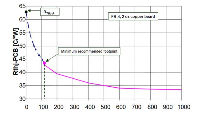
How can I achieve good heat rejection of Power MOSFET CSD19535KTT with D2PAK package?

While comparing to the base area of MOSFET, I am increasing the copper area on the PCB like 10%, 20%, 30% and so on.

while doing like that when i can get the good heat rejection point? Also i wanted to know how i can find the saturation point of heat rejection when we go on increasing the area of copper deposited on the PCB.

what are the effects of Heat transfer when the area of copper on the pcb is increasing?

Regards,

Jnaneswar 

  • Jnaneswar,

    Thanks for your interest in our MOSFETs.

    On our webite at this link :

    , there are a host of resources that you may find useful.

    There is one particular technical  article that should be of particular interest to you and is the one titled " Selecting the right power MOSFET/power block package for your application"

    This article goes into typical power dissipation capabilities of various MOSFET packages in a typical application. However, as discussed in the article please remember the amount of power a MOSFET can dissipate is very much dependent upon the individual pcb design and thermal environment. The more airflow, the more vias, the more pcb layers, the thicker the copper all mean the lower the thermal resistance of the pcb and the more you can dissipate into your pcb.

    I hope this helps

  • Chris,

    Thanks for providing useful information, but can I get in detail if i increase the copper area on the top layer of my FR4 PCB when compared to the Tab area of MOSFET, How the heat flow is getting to be effected? Can you suggest any application notes from TI that can be referred?

    Regards,

    Jnaneswar. 

  • Jnaneswar,

    Unfortunately there are no application notes I am aware of from TI.

    I did a quick search on the internet and came across this paper that may be of use from the IEEE.

    The other way to accomplish this is to use a thermal modelling software like FloTHERM.

  • Chris,

    The paper which you suggested in the previous reply, they considered the thermal vias in their case. But i wanted to know the effect of copper solder area under the Tab of the MOSFET without considering thermal vias. Can i get the information about the effect of copper solder area by consideration of vias and without consideration of vias is same?

    Regards, 

    Jnaneswar 

  • Jnaneswar,

    I managed to locate some data that shows thermal resistance, junction to pcb, vs drain pad area on a single layer FR4 board with 2oz Cu layer. Area on x-axis is in mm2.

  • Chris,

    I am unable to view the file which you sent in the last reply. Can i get a clear view of that file?

    Regards, 

    Jnaneswar

  • Jnaneswar,

    Hopefully you can read this image.

  • Chris,

    Thank you for the valuable information.

    Best Regards,

    Jnaneswar