This thread has been locked.

If you have a related question, please click the "Ask a related question" button in the top right corner. The newly created question will be automatically linked to this question.

TPS92513: Start up behavior

Part Number: TPS92513

Hi expert,

My customer have an question for TPS92513 startup behavior.

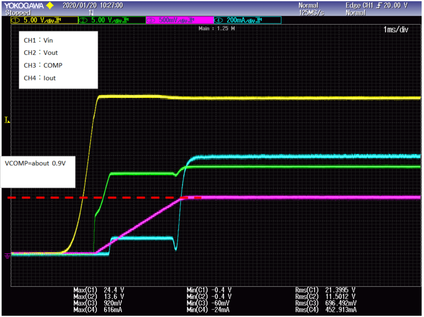
Could you please let me know the reason of the following behavior that is output current was leaked a little at startup?

Thanks

Muk

  • Hello,

    Is this during initial turn-on or a power cycle?  Is COMP partially charged during turn-on from a previous power on?  Can you look at the switch node during this time?  What is PDIM doing during this time?

    Best Regards,

  • Hi Irwin-san,

    Thank you for your supporting

    >Is this during initial turn-on or a power cycle?

    Initial turn-on

    > Is COMP partially charged during turn-on from a previous power on?

    Please refer the following waveform.

    > Can you look at the switch node during this time?

    Please refer the following waveform.

    >What is PDIM doing during this time?

    Open

    -

    Thanks

    Muk

  • Hello,

    During start up the TPS92513 runs in minimum pulse width to charge the LED bypass capacitor:

    From The Datasheet:  "8.4.1 Start-Up
    To reduce inrush current and to keep the regulator in control during all startup conditions the TPS92513 employs
    a startup mode that behaves differently than during normal operation (regulation mode). The UVLO conditions
    must be satisfied before the TPS92513 is allowed to switch. When the UVLO pin is held low the device enters a
    low-power shutdown mode, and some internal circuits are deactivated to conserve power. When UVLO returns
    high these circuits are enabled, which results in a delay of approximately 50 μs (typical) before switching starts.
    During start-up the TPS92513 operates in a minimum pulse width mode which is an open-loop control. At the
    start of each switching cycle the internal oscillator initiates a SET pulse. The high-side MOSFET turns on with a
    minimum pulse width of 140 ns (typical), independent of the COMP voltage. The device does not pulse skip.
    While operating in minimum pulse width mode, the LED bypass capacitor is being charged causing an in-rush
    current. Also, the COMP voltage begins to rise as the error amplifier output current charges the compensation
    capacitor. When the COMP voltage reaches approximately 0.7 V, the error amplifier is ensured to be out of
    saturation and to have sufficient gain to regulate the loop. The TPS92513 then transitions from minimum pulse
    width mode to regulation mode. During regulation mode the error amplifier is now in closed-loop control of the
    system. The gain of the error amplifier quickly increases the duty cycle, which causes the output voltage to
    increase. Once the output voltage approaches the forward voltage of the LED string, the LED current quickly
    begins to increase until it reaches regulation.
    There is a slight delay from the time the VIN and EN UVLO conditions are satisfied until the time the error
    amplifier has control of the feedback loop. This delay is a result of the time it takes COMP to charge the
    compensation capacitor to 0.7 V. This delay can be approximated as shown in Equation 10."

    Best Regards,