This thread has been locked.

If you have a related question, please click the "Ask a related question" button in the top right corner. The newly created question will be automatically linked to this question.

BQ25898: Charger Input power good detection is faulty

Part Number: BQ25898

Hi,

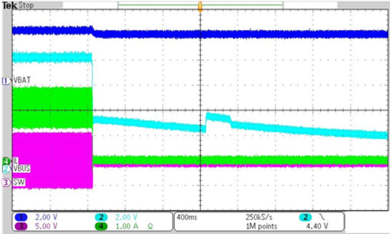
We came across a problem on some of our production units where the device input voltage is still present even after charger input is removed which results in faulty indicator.

Anyone seen this problem before?

thanks

  • Hi Hank,

    The purpose of the reverse blocking FET (RBFET) Q1 is to prevent this from happening when exiting charge mode and entering sleep/HiZ mode.  Just to confirm, you have not accidentally entered OTG mode?  Is OTG pin low or high?  Is OTG enabled in I2C register?  Is there a squarish waveform at SW?

    Regards,

    Jeff

  • Hi Jeff,

    the OTG pin is tie to ground through a 10K resistor. 

    OTG bit on register 03 is untouch and should default to disable

    there is no waveform on the SW node. only a DC voltage from the battery. Note that this measurement is with the charger NOT connected.

    thanks

  • Hi Jeff,

    please note that we have added a RC filter at the SW node to dampen the ringing because we had issues with radiated noise in the cellular band. I believe this was suggested by TI.

    thanks

  • Hi Jeff,

    when the charger is plugged in, we do have a square wave. please see attached for picture.

    thanks

  • Hi Jeff,

    do you see any issues with this SW cct.

  • Hank,

    I don't see any issues with the SW pin circuitry, other than the series resistor with BTST capacitor is higher than I have ever seen.  5 ohm is the highest that I have seen.

    Regards,

    Jeff

  • Hank,

    Could you please provide all BQ25898 register values?

    Thanks,

    Ning.

  • Hi Jeff,

    yes, that seems to be the problem. What does BTST pin control? why does this series resistor cause this problem?

    thanks

  • Hi Jeff,

    any update on this? Urgent as production has stop pending an understanding of why this is happening.

    thanks

  • Hank,

    In order to understand the behavior, could you please provide all BQ25898 register values?

    Thanks,

    Ning.

  • Hi Ning,

    our FW guys says that he has not way of reading all registers. here is what he got. 

    REG04  0x25

    REG05 0x15

    REG07 0x8B

    REG09 0x54

  • Hank,

    It looks like you have a workaround already. We do not have enough information (such as all the register values etc) to make any conclusions so far.

    Thanks,

    Ning.

  • Hi Ning,

    Unfortunately we don't understand why changing the series resistor on BTST pin makes the problem go away on some units. We have already shipped out lots of units with a 10 ohm value and this value do work on some units. I am worried that this will cause problem with the units out in the field so I would like to understand what the BTST pin does and why some units depend on the resistor value. can you shed some light on this. 

    Is there a software solution for the devices we shipped?

    Please let me which registers you are interested in and how to get it. I will ask our FW guys.

    thanks

    Henry

  • Henry,

    The following info would be helpful:

    1. When "the device input voltage is still present even after charger input is removed", please take VBUS, SW, VBAT and I_inductor waveforms. I_inductor gives idea about the load condition when charger input is removed.

    2. What is the operating charger input voltage before it is removed?

    3. Actual VINDPM threshold. Related registers are REG0D AND REG01[0].

    Thanks,

    Ning.

  • Hi Ning,

    I will get you the answers today.

    I have another questions regarding the units out in the field with the 10 ohm series resistor. Is it save to say that if they work at room temperature, that they should be working over temperature and time? we are try to determine if we should recall them.

    thank

    Henry

  • Hi Ning,

    1) please find the captures of VBUS, VBAT, VSYS, and SW node. 

    2) the input charger voltage is 12V

    3) we have implemented VINDPM to set the input range to be at 5V which is higher than the VBAT, we are still getting the same fault.

    Here are the images with charger removed:

    Fig 1. SW node with charger removed

    SW node with Charger Unplugged

    Fig. 2 VBAT with charger removed

    VBUS with Charger Unplugged

    Fig.3 VBUS with charger removed

    Fig 4. VSYS with charger removed

    let me know if you want images with charger plugged in.

    thanks

    Henry

  • Henry,

    Could you please lower the VINDPM setting from 5V down to 3.9V and check if the behavior happens or not?

    Thanks,

    Ning.

  • Hi,

    We haven't heard from you for a while. The thread is considered solved and closed.

    Thanks,

    Ning.

  • Hi Ning,

    this is NOT resolved yet.

    I will get you an answer to your question regarding setting VINDPM to 3.9V in a couple of days.

    I am still waiting for your answer regarding why the series resistor value at BTST pin makes a difference. 

    thanks

    Henry

  • Henry,

    As stated earlier, we do not have enough information to make any conclusions yet. Please provide the data requested and we will do our best to investigate.

    Thanks,

    Ning.

  • Hi Ning,

    we have changed the VINPDM setting to 3.9V and still having the same problem.

    Henry

  • Hi Hank,

    If the charger is switching with battery only and OTG is turned off, then it is boosting back to the input (unintentional OTG).  We have seen this before with very high (>100 ohm) series resistance with BTST that was due to poor layout but never with only 10 ohm series resistor to reduce EMI.  Also, it is odd that changing VINDPM did not stop the boost back.  Since lowering the resistance stops the problem, I will assume this case is closed.

  • Hi Ning,

    It is odd that only some devices behave this way with 10 ohms and some still OK with 24 ohms. So you are saying some of the devices in this lot is defective? 

    I am not sure if this case is resolved yet. If we are to put the series resistor to 0 ohm, I am worried that EMI will be an issue as we put this series resistor to lower it in the first place.

    when you say boosting back(unintentional OTG), what exactly is this mean? can you explain it in more detail?

    thanks

    Henry

  • Hi Henry,

    If the buck converter is synchronous (low side FET instead of diode), there is the possibly for negative inductor current to flow, even when operating in buck mode.  When you connect a synchronous buck converter in reverse (i.e. a power source at the output and floating or load at the input), as a battery charger will be when no input power is applied, there is a risk of negative inductor current flowing back to the input, so called boosting back to the input.  With adapter applied at the input for buck mode, we add special circuitry to limit the reverse current flow to prevent boost back during buck mode.  Now, because the charger uses a high side NFET, instead of PFET, it needs the BTST 1/2 charge pump circuit to provide the drive voltage for the NFET.  At light load, the charger must force a refresh pulse to keep that BTST capacitor charged.  If the resistance in the BTST trace is too high, the refresh pulse occurs more frequently.   With no resistive load on PMID or VBUS to discharge their capacitors, the charger can set up a self sustained loop where VBUS stays higher than UVLO and the refresh pulse continues. The VINDPM threshold can usually be changed to prevent this from happening.  Apparently, your board's BTST trace resistance and lack of load on VBUS or PMID sets up  the "perfect storm" for boost back.  Is the trace from BTST pin to capacitor to SW highly resistive, even without the series resistor, or using single VIAs to connect through board layers?  Does adding a load (like 10kohm) on VBUS to pull VBUS below UVLO stop the boost back?

    Regards,

    Jeff 

  • Hi Jeff,

    thanks for the explanation.

    -do you have a sense why most of the devices are OK even with a much higher resistor values then 10 ohms while some don't work at 10 ohms? 

    -we did short the VBUS pin to ground to stop this problem although we didn't try 10k.

    -the connection SW and BTST is quite short with a relatively wide trace. see attach picture on the layout. 

  • Hi Hank,

    You are only the 3rd customer of hundreds (who buy multi-millions of units) who have seen this issue with this product family.  Are you certain that the resistors installed were 10ohm and not 100 ohm or more?  The resistor trace appears to use single vias.  Via impedance varies greatly even on the same pcb.  Unfortunately, we have no way to test BTST impedance in production and do all of our validation without a series BTST resistor.

    Regards,

    Jeff

  • Hi Jeff,

    I am quite sure it is 10 ohms. yes the layout is using a single via. I can measure the resistance of this via. What is the maximum resistance tolerated?

    question on the operation of the device: Shouldn't RBFET prevent the voltage at the output getting back to the input?

    thanks

    Henry

  • Hi Henry,

    The max resistance hasn't been measured but based on experience with other devices using this topology and the other customer failures on this device, I would say <<20 ohm.

    The RBFET is controlled by comparators that compare battery voltage and VBUS voltage.  Because VBUS is staying above VBAT+80mV (sleep threshold) due to unintentional OTG, the RBFET stays on.

    Regards,

    Jeff

  • Hi Jeff,

    We are stil not given up a software solution for the bad units out in the field. Is there something else you can suggest other than setting the VINPDM voltage? How can I be sure that OTG is disabled?

    thanks

    Henry

  • Henry,

    Unfortunately, other software workaround is not available. You may try higher quality BTST capacitor with lower leakage current or keep BTST resistance minimum and focus on EMI reduction by adding EMI bead etc.

    Thanks,

    Ning.

  • Hi Ning,

    I am not sure if we set the VINPDM correctly, how can I test this to make sure? 

    can I just vary the charger voltage and probe the PG status?

    thanks

    Henry

  • Henry,

    Please take VBUS, SW, VBAT and I_inductor waveforms as below when VBUS is removing and check at what VBUS voltage the device stops switching.

    Thanks,

    Ning. 

  • Hi Ning,

    I have tested a device which had the VINPDM set at 5V, it does not seem to behave the way I thought it would. When I lowered the charger voltage to 4.2V, I still see switching at SW node. I thought it would not switch below 5V. 

    thanks

    Henry

  • Hi Jeff, Ning,

    I have another unit that was working fine with the 10 ohms series resistor and now I retested it and it shows that same problem. I changed the resistor to 0 ohm and still doesn't work. now I removed the charger chip so that I can get access to the  pins to measure the traces resistance as you were saying that the layout might be an issue. I measured <0.5 ohm on both traces connecting to the chip.

    I am not sure how to proceed with this problem. Please give me some guidance.

    thanks

    Henry

  • Henry,

    The device may switch when VBUS is from 3.9-V to 14-V. Please set VINDPM to the minimum 3.9V.

    Have you tried high quality BTST capacitors with lower leakage current? On the EVM, 2kohm BTST resistor needs to be added to simulate a leakage path in order to produce the behavior.

    500mohm is relatively high. The best solution is to redo the layout.

    Thanks,

    Ning.

  • Hi Ning,

    I don't understand that you need 2K to produce this behavior and yet you are saying <0.5 ohms(it is actually less because the probe has resistance. I think it is more like 0.2 ohms) would be an issue.

    Is it possible to use VINDPM setting to solve this problem? if so, how can I test whether our FW guys is programming this register correctly?

    thanks

    Henry

  • Henry,

    1. As mentioned earlier, setting VINDPM to the minimum 3.9V usually helps. i.e. set FORCE_VINDPM bit  (REG0D[7]) to 1 and REG0D[6:0]=0001101 (3.9V). Please read back REG0D to make sure 3.9V VINDPM is set correctly.


    2.  The BTST resistor is to simulate a leakage path. What's your BTST capacitor value and voltage rating? Is it high quality ceramic cap? The official EVM uses Murata GRM155R71E473KA88D, CAP, CERM, 0.047uF, 25V, +/-10%, X7R.


    Thanks,

    Ning.

  • Hi Ning,

    1. I will have our FW guy check the register. 

    How do I test to make sure that it is programmed properly?

    how does VINDPM work?

    Is my understanding that if VINDPM is set to say 5V, then it would not charge with input lower than 5V?

    2. we are using the exact same part for the cap.

    thanks

    Henry

  • Henry,

    For VINDPM operation, please refer to 9.2.6.2 Dynamic Power Management and 9.2.3.4 Input Voltage Limit Threshold Setting (VINDPM Threshold) on the d/s for the details.

    To verify VINDPM threshold,

    1) Read back REG0D and it should be 10001101.

    2) Take VBUS, SW, VBAT and I_inductor waveforms when VBUS is removing as the sample waveform provided in the earlier response.

    Thanks,

    Ning.

  • Hi Ning

    We've check the setting again and seems to be correct and it is not helping in terms of this problem.

    Is it possible for me to send you some bad ICs to analyze why it is not behaving the way we expected?

    thanks

    Henry

  • Henry,

    Could you please add a 10kohm resistor from VBUS pin to GND and check if it helps?

    Thanks,

    Ning.

  • Hi Ning,

    It does NOT help. I tried many different values as low as 1K and still does not work.

    thanks

    henry

  • Henry,

    Could you please try your problematic ICs on a working BQ25898 EVM and see if it behaves the same?

    Thanks,

    Ning.

  • Hi Ning,

    I cannot successfully desolder the IC from a board and resolder it onto the EVK.

    Henry

  • Henry,

    Could you please find any internal or external soldering resources to help you?

    Thanks

    Ning.