This thread has been locked.

If you have a related question, please click the "Ask a related question" button in the top right corner. The newly created question will be automatically linked to this question.

WEBENCH® Tools/TPS54202: Whats the proper schematic and layout to pass FCC sDoC for TPS54202?

Part Number: TPS54202
Other Parts Discussed in Thread: TIDA-00947, TIDA-00949

Tool/software: WEBENCH® Design Tools

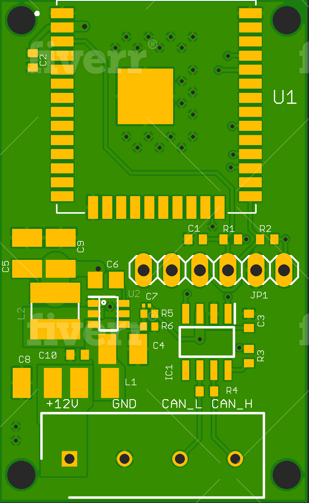
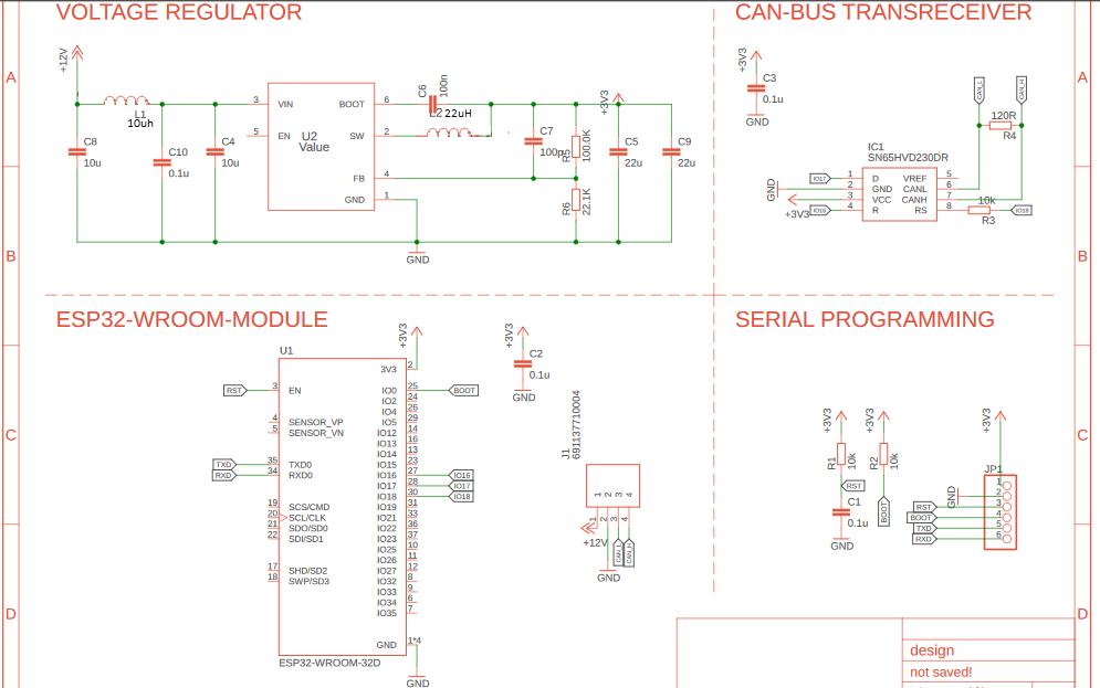
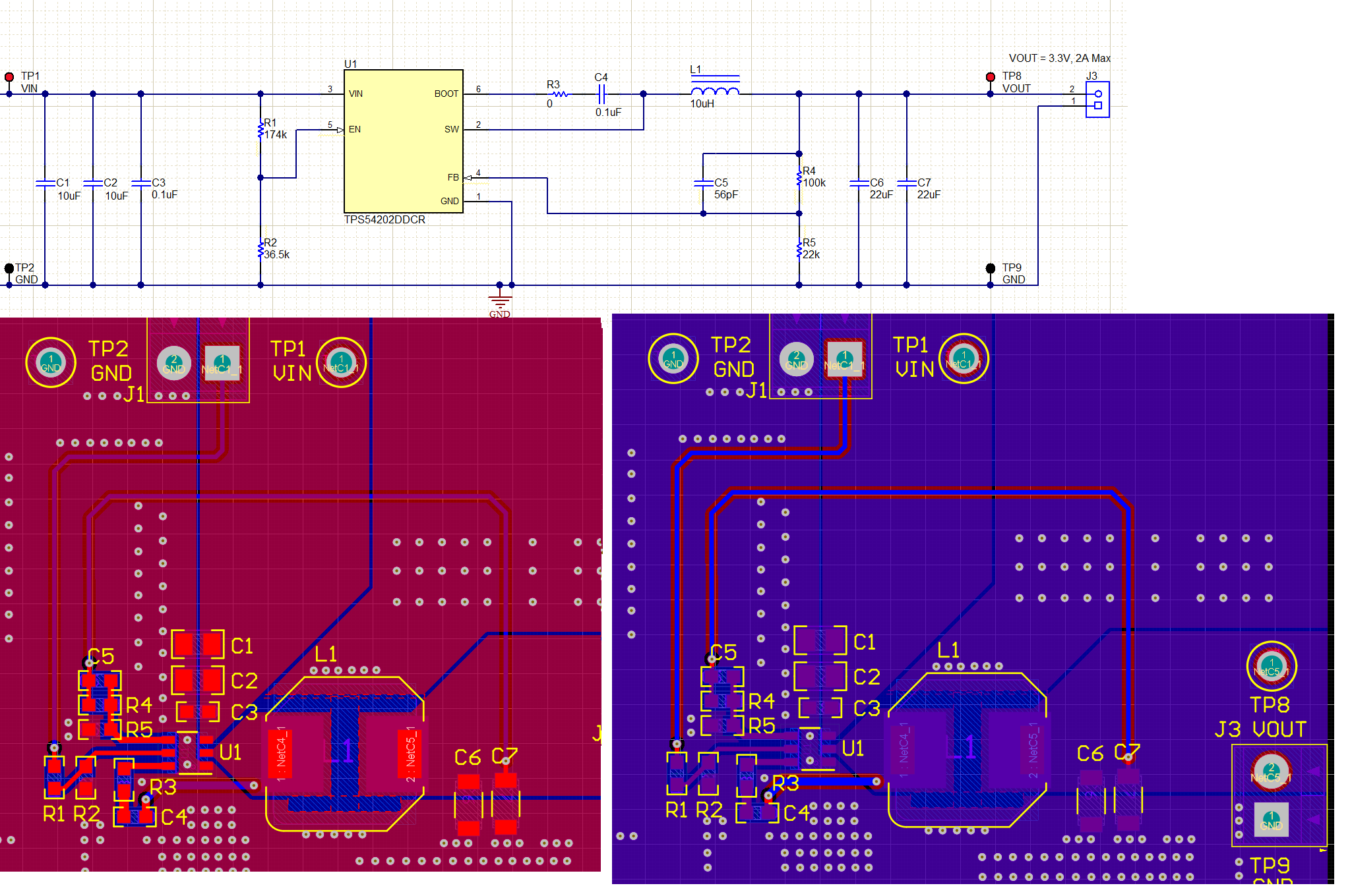
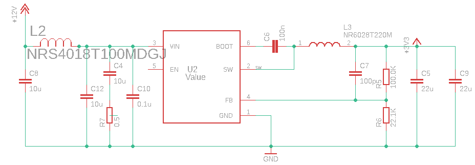
Hi Im begginer in switching power supplies. I need switching regulator which would pass FCC sDoC. In datasheet I find one advised layout of pcb, in webench design tool I get way different pcb layout. Now I found TIDA-00947 which uses TPS54202, it gives way different schematic than webench (different resistor values for fb pin + input  filters to pass conducted emision tests). I got confused a lot. I was hoping someone could help me or direct to choose proper schematic + layout for passing FCC sDoC. My input voltage is 14V battery, output needed 3.3v, current 0.1-0.5A, Ill be powering esp32-wroom module and using bluetooth.

  • hi,

    if your PCB size has no limitation, use layout suggestion in datasheet.  You can upload your schematic and layout to review for you.

  • Hi, it has some size limitations, thats why Ive decided use schematic/layout similar to https://www.ti.com/tool/TIDA-00949. Can you check layout please and let me know what you think?

  • Former Member
    0 Former Member in reply to Deividas Seip

    Hi Deividas,

    Could you please directly attach your schematic/layout files at this topic? Public file sharing services are blocked by TI policy. I cannot get the access to your uploaded files in the Cloud.

    I just attached a reference layout as below:

    Thanks.

  • layout+schematic.rarHi, I hope this format is enough.

  • Former Member
    0 Former Member in reply to Deividas Seip

    Hi Deividas,

    Please check my inputs below:

    1. C6 should be connected between BOOT pin and SW pin, while in your schematic it is connected between BOOT pin and output terminal.

    2. Add an electrolytic capacitor as damping device in the input capacitor side. You can refer to the app notes for detailed design process: http://www.ti.com/lit/an/snva489c/snva489c.pdf

    3.  As for layout, please refer to my attached capture as below:

    a. Keep C10 as close as possible to the VIN and GND pins (The same as capture below of C3)
    b. Both feedback resistors, R5 and R6 must be located close to the FB pin. Place C7 directly in parallel with R5. If VOUT accuracy at the load is important, make sure VOUT sense is made at the load. Route VOUT sense path away from noisy nodes and preferably through a layer on the other side of a shielded layer.

    Thanks.

  • Thanks for you time to check. It looks I will have rework my layout completely. Ill try to copy your provided layout. Any chance you could provide me schematic for your used layout? Also do I need electrolytic capacitor as filter, because TIDA-00949 shows it can pass emission test with small filter L+C (L=5uH, C=10uC) and I need to save space?

  • Former Member
    0 Former Member in reply to Deividas Seip

    Hi Deividas,

    Please find my schematic and layout files from the attachment, and I used Altium Designer for the layout. 

    As for the additional LC input filter, I recommend adding one 47uF electrolytic cap in case any stability issue. Or to save space, a ceramic capacitor in series with a small resistor can be a good choice.(

     TPS54202EVM.zip

    . A ceramic capacitor in series with a small resistor can be a good choice.

  • Hi, I have adjusted my schematic and added damped filter, I think it should be enough filtering.

    1.Just I want your opinion will it be stable? 2. Do I need C12?     L2=10uH, L3=22uh; R7=0.5ohm;

  • Former Member
    0 Former Member in reply to Deividas Seip

    Hi Deividas,

    Please check my inputs below:

    1. It is OK, and you can start from this. I would like to recommend leaving the place for the C4 and R7, and adjust the value according the test results.

    2. C12 is needed and should be placed close to VIN pin and GND pin. C10 should be placed as close to VIN pin and GND pin too.

    3. C7=100pF also can be adjusted to 56pF.

    Thanks.