This thread has been locked.

If you have a related question, please click the "Ask a related question" button in the top right corner. The newly created question will be automatically linked to this question.

BQ76942: Role of Additional FET in Discharge FET Drive Circuit

Part Number: BQ76942
Other Parts Discussed in Thread: BQ76952,

Hi!

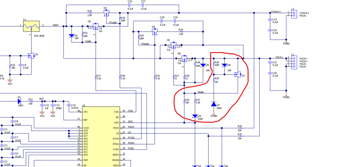
I was looking through the "Parallel Paths with the BQ76952 Battery Monitor Family" application note (http://www.ti.com/lit/an/slua952/slua952.pdf) and in the Parallel FET Schematic (page 3), I'm curious what this part of the circuit does/what are the complications of omitting this.  
Thanks in Advance!

  • Hi Ishaan,

    Thanks for asking this. I realize now that this is not discussed in our documentation, so we will try to make this more clear in the future.

    This circuit is for reverse charger protection. The evaluation module is normally populated for series FET configuration and the charger would normally connect to PACK+/PACK- pins. Many applications require protection for the charger being connected backwards. If this is not needed on your system, there is no problem removing this circuit.

    Best regards,

    Matt

  • Okay, makes sense! Should a series ~5.1K resistor still be added between the DSG pin and the gate of the NFETs in the discharge path, even in the case of paralleling multiple FETs in the discharge path?

    Thanks in advance! 

  • Hi Ishaan,

    While the circuit is called a "reverse charge" circuit it will also turn on in case of a short circuit and an inductive path of the short.  When PACK+ goes negative the circuit will turn on and clamp the discharge FET off stopping the current quickly.  You may or may not want that.

    There should be a resistance between the BQ76942 pin and the gate of the FETs, R25 if using a symmetrical turn on/off or R25 & R27 if using a faster turn off circuit as shown. (The asymmetrical turn on/off also allows limiting the current in/with R25 during reverse charge).  The minimum suggested is 100 ohm, RGATE used in the High-side NFET Drivers section test conditions. 

    Use a resistance or ferrite bead in the individual gate path with parallel FETs (R23, R26 above) to avoid oscillation.  Some literature recommends the individual gate resistance be about 10% of the total, certainly it needs to be large enough to suppress the oscillation.  Refer to your preferred design reference material on FETs for guidance.