This thread has been locked.

If you have a related question, please click the "Ask a related question" button in the top right corner. The newly created question will be automatically linked to this question.

BQ25895: Input current lower than expected.

Part Number: BQ25895
Other Parts Discussed in Thread: BQ25890

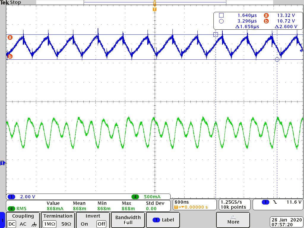
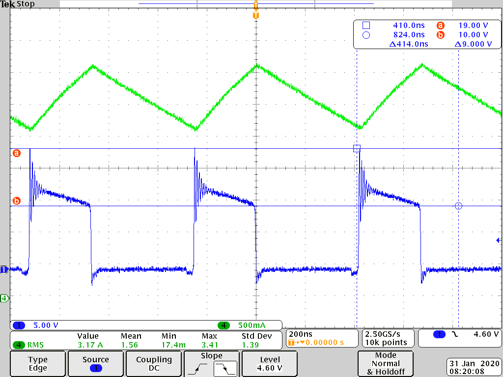
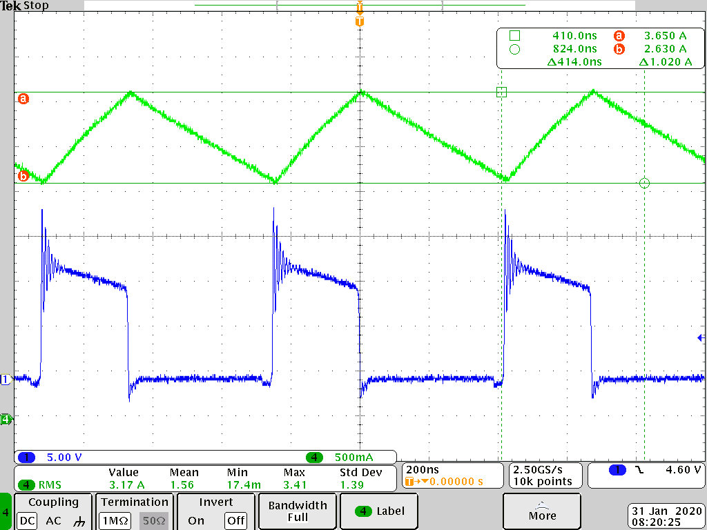
I've been testing the BQ25895 and we have set Reg04 to the maximum 5A limit (0x4F).  Battery voltage is 3.6V.  Ilim pin is has a 215ohm resistor on it which limits input current to 1.6A.  Whenever I charge with a 2.4A, 5V adapter I get 8 watts of power, which is about what I would expect.  With the maxcharge adapter I only get 13W of power.  I've confirmed the adapter is outputting 12V.  I previously measured input voltage drop and it is about 400mV total at 2Amps, so I know that is reasonable given the constraints of most USB cables.  I would expect about 18W with a maxcharge adapter. 

Any thoughts on what might be the issue?

  • Hi Andrew,

    The BQ25895 can limit input current either at power up using the D+/D- pins, by IINDPM (input current limit), ILIM pin resistor (clamps to lower of the this setting or IINDPM register), VINDPM (input voltage droop prevention) or thermal regulation.  When you attached the 12 V adapter, what input current limit did the charger auto select for the IINDPM registers?  Is the charger status register reporting thermal regulation?

    Regards,

    Jeff

  • Hi Jeff,

    REG0B reports a Maxcharge Adapter for the 12V.  We are working on a command to dump all the registers so we can review them all.  I got out a Oscope current probe and measured 1.2Arms current with the 5V adapter and 0.9Arms current for the 12V.  So neither one is really matching up to what I would expect.  I also noticed that the Ilim pin reads 0.572V for 5V and 0.385V for 12V with a 215ohm 1% resistor there.

    I'll update you once I have a dump of all the registers.

    Thanks,

    Andrew

  • Hi Andrew,

    Just to confirm, the charger will only pull the amount of input current it needs for the load current pulled from SYS plus the charge current.  At higher input voltages, for the same load current, the input current drops but the total input power increases but efficiency decreases.  Are you getting your desired SYS load current plus charge current?

    Regards,

    Jeff

  • Jeff,

    I'm charging a half charged battery and also adding extra load with some LM317s on a heatsink configured for constant current mode.  I see no increase in input current when I add additional load.  Below are the registers:

    12V Charger

    BQ25895 Reg00 = 0x5c
    BQ25895 Reg01 = 0x5
    BQ25895 Reg02 = 0x3d
    BQ25895 Reg03 = 0x3a
    BQ25895 Reg04 = 0x20
    BQ25895 Reg05 = 0x13
    BQ25895 Reg06 = 0x5e
    BQ25895 Reg07 = 0x9d
    BQ25895 Reg08 = 0x3
    BQ25895 Reg09 = 0x44
    BQ25895 Reg0A = 0x93
    BQ25895 Reg0B = 0x96
    BQ25895 Reg0C = 0x80
    BQ25895 Reg0D = 0x58
    BQ25895 Reg0E = 0x0
    BQ25895 Reg0F = 0x0
    BQ25895 Reg10 = 0x0
    BQ25895 Reg11 = 0xe2
    BQ25895 Reg12 = 0x0
    BQ25895 Reg13 = 0x13
    BQ25895 Reg14 = 0x39

    5V Charger

    BQ25895 Reg00 = 0x7f
    BQ25895 Reg01 = 0x5
    BQ25895 Reg02 = 0x3d
    BQ25895 Reg03 = 0x3a
    BQ25895 Reg04 = 0x20
    BQ25895 Reg05 = 0x13
    BQ25895 Reg06 = 0x5e
    BQ25895 Reg07 = 0x9d
    BQ25895 Reg08 = 0x3
    BQ25895 Reg09 = 0x44
    BQ25895 Reg0A = 0x93
    BQ25895 Reg0B = 0x76
    BQ25895 Reg0C = 0x80
    BQ25895 Reg0D = 0x13
    BQ25895 Reg0E = 0x0
    BQ25895 Reg0F = 0x0
    BQ25895 Reg10 = 0x0
    BQ25895 Reg11 = 0x98
    BQ25895 Reg12 = 0x0
    BQ25895 Reg13 = 0x5b
    BQ25895 Reg14 = 0x79

  • Below are your settings at 12V

    and 5V:

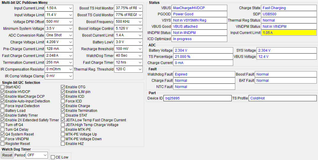
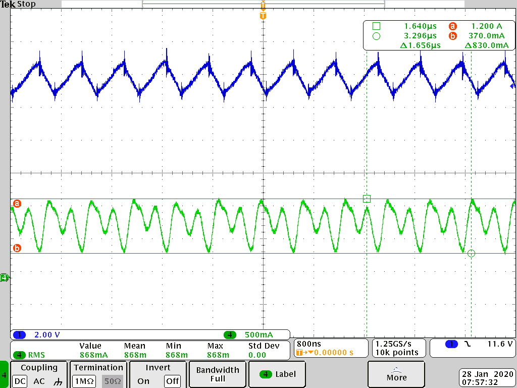
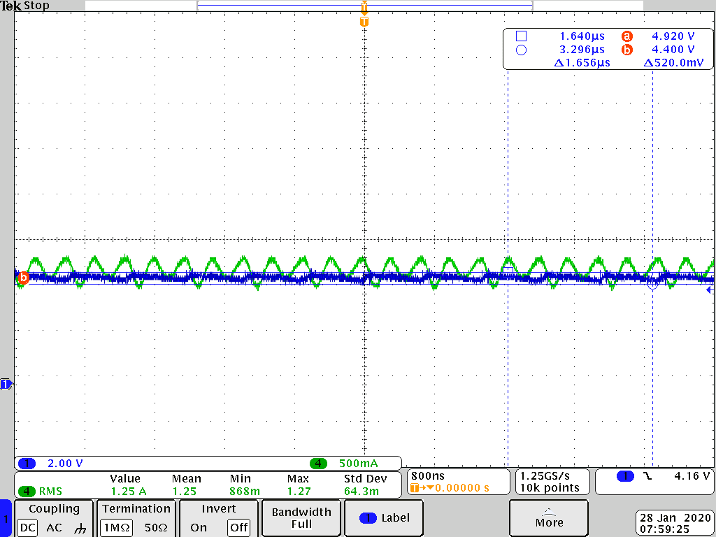
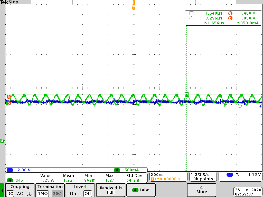
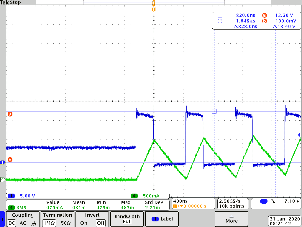
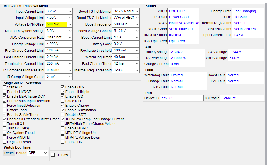
     In both cases, relative VINDPM and ICO/ICD are enabled.  Even though in the 12V HVDCP case, IINDPM reg is set to 1.5A, the ICO/ICD routine determined that the input power source or connector or cable is too resistive, causing the voltage at VBUS to droop below the VINDPM value of 11.4V. The ICO/ICD routine has limited the input current to 1.05A. But, there is still enough input power for your SYS load plus charge current because none of the DPM loops are active.  However, for the 5V DCP adapter, IINDPM is at 3.25A but ICO/ICD  has limited the input current to 1.45A and the charger's IINDPM loop is active when means there is not enough input power for the system load plus charge current and charge current is reduced.  If you can't make your input source+connector+cable less resistive, you can change to absolute VINDPM using the force VINDPM and lower the VINDPM threshold and/or you can disable ICO/ICD. 

    Regards,

    Jeff

  • Jeff,

    That makes sense.  We also figured out the watchdog was resetting our register values.  We went ahead and disabled the watchdog. 

    Now I'm seeing other issues.  The 12V QC adapter when plugged in would start to charge for 10s of milliseconds and then quit.  It would then retry every 4.6 seconds over and over.  It then finally kicks in after about 20 tries and draws the expected 18 watts, but then after awhile it started drawing 25 watts.  The adapter is only rated for 1.5A.  The 25895 got pretty hot.  I checked the registers and don't see why it would be drawing this much.  I also noticed the input voltage ripple is 4V which seems really high, when it charges from 12V.

    BQ25895 Reg00 = 0x5c
    BQ25895 Reg01 = 0x5
    BQ25895 Reg02 = 0x3d
    BQ25895 Reg03 = 0x3a
    BQ25895 Reg04 = 0x4f
    BQ25895 Reg05 = 0x13
    BQ25895 Reg06 = 0x5e
    BQ25895 Reg07 = 0x8d
    BQ25895 Reg08 = 0x3
    BQ25895 Reg09 = 0x44
    BQ25895 Reg0A = 0x93
    BQ25895 Reg0B = 0x96
    BQ25895 Reg0C = 0x80
    BQ25895 Reg0D = 0x59
    BQ25895 Reg0E = 0x0
    BQ25895 Reg0F = 0x0
    BQ25895 Reg10 = 0x0
    BQ25895 Reg11 = 0xe3
    BQ25895 Reg12 = 0x0
    BQ25895 Reg13 = 0xc
    BQ25895 Reg14 = 0x39

  • Hi Andrew,

    I don't see why the IC would be restarting from the registers.  In fact the ICO/ICD has reduced current to 700mA which is even less power.  Do you have an oscilloscope with current probes in order to capture VBUS, IBUS, VSYS, ISYS or IBAT while cycling and again after it stops cycling?  Can you replace the adapter with a bench power supply at 12V and limited to 1.5A output and repeat?

    I noticed that your charge current is set to 5A.  In order to achieve 5A charge current you need lots of ground heat sink area for the IC.  Otherwise, the IC will go into thermal regulation and scale back the input current further. 

    Regards,

    Jeff

  • Jeff,

    I went back and changed the max fast charge current back to 2.048A.  Below are the scope shots of a 12V QC3.0 Adapter and a 5V 2.4A adapter.  Yellow is Vsys and Green is the current on Vsys.  The system is of so all the current is going to the battery.

    12V QC3.0

    5V, 2.4A Adapter

    The input ripple is pretty bad with the QC3.0 adapter.  I'm assuming this is because we are limited to 1.0uF of input capacitance.  It seems like an a lot, any DC-DC I've designed has always had much less.

    I'll go back and capture the same with the charge current set to 5amps.  I'm a bit concerned that it was overloading the 12V adapter, the adapter is rated for 18W and it was drawing 25watts.  It should have limited to 1.5A regardless, but I did not see this behavior and the BQ25895 got very hot under these conditions and it appeared to go into thermal shutdown.

  • Andrew,

    Can you send your schematic and layout files?  TI uses Altium for layout but layout of each layer in PDF is okay.

    Regards,

    Jeff

  • Jeff,

    I believe the issue is the inductor is saturating and causing all the other control loops to work improperly.  I tried backed charge current from 5A down to 4A and things still misbehaved.  I then went to 3A and things started to work as expected with the 12V adapter.  This also explains why the part was going into thermal protection since the high side switch was outputting more current due to the drop in inductance.

    The inductor I specified looks like it should be OK per the datasheet even with a 5A charging current, but obviously it it is saturating sooner than expected.

    https://ds.yuden.co.jp/TYCOMPAS/ut/detail?pn=NRS8040T2R0NJGJ%20%20&u=M

    I replaced with this inductor with a larger one just to experiment and it does work at 5A.

    https://www.digikey.com/product-detail/en/w-rth-elektronik/7843340220/732-11776-1-ND/8134480

  • Jeff,

    With the charge current set to 5A I still see some issues even with a higher sat. current rated inductor.  So I'm thinking that isn't the entire root cause.  Even with a larger inductor when the charger starts to charge a discharged battery, it seems like it starts switching and then shuts down immediately and then retries 5 seconds later and just keeps repeating.  So I'm not sure what is going on.  If I reduce the charge current set point to 3 amps it always starts up fine and draws the expected 18-19 watts.  I can send you schematic and the other requested info, but I would rather email it to you.  Can you friend me on here and I then send me your email via PM?

  • Jeff,

    Here are some pictures of the inductor current while it is charging with a 3Amp limit.  Blue is the switch node and green is inductor current.  It still does this weird shutdown where it stops charging for 30 seconds and then charges for a few minutes and turns back off for 30 seconds.  I'm watching the IC temperature and it is only getting to 65-70C according to the thermal imager.

    This is what it looks like when it stops charging for 30 seconds

  • Andrew,

    The SW node waveform has a steep slope which implies high resistance somewhere.  Are the register values that your previously provided from the period when the charger is operating correctly or when it is not charging?  I need to see the registers when it is charging and not charging including the ADC measurements.  Also, can you provide scope shot of VBUS, IBUS or IL, VBAT and IBAT and also VBUS, IBUSor IL, VSYS and ISYS that shows the when the charger stops and starts switching? 

    Regards,

    Jeff

  • Ok, I'll work on getting those to you.  I've got to discharge the battery all the way down again.  I agree, that Vin has a lot of voltage drop.

    There is 0.250 Ohms on Vbus and 0.150 Ohms on ground from the USB A connector on the cable to the Vin pin/Gnd pin using a 3 foot, 23awg USB cable.

    As far as the claimed "thermal regulation" goes, shouldn't the device just reduce the charge current rather than turning off if it was getting too hot?  The part acts like it is going into a  thermal shutdown rather than regulation which the term "regulation" would imply a control loop.  I can make the time when the part is not charging much shorter if I just blow air on the part with my mouth.  It seems like it behaves more like a comparator than a control loop with, at minimum, an integrator and maybe a proportional term.

  • While waiting for the battery to discharge, I did a voltage drop measurement on a second PCB.  With 1.5A on Vin, I measured from the male end of the USB A connector to the Vin pin on the BQ25895.  I measured 0.46V of drop.  I measured USB A ground to PCB ground and measured 0.23V.  This still doesn't explain the nearly 3V of drop when the high side switch is turned on.

  • Andrew,

    That seems indicate that your board has a grounding issue.  How are the IC powerpad and PGND pins connected?

    Regards,

    Jeff

  • Pads are turned off so you could see the vias.  There are two internal layers that are just ground plane.

  • Are the capacitors on the PMID pin required if we are not using the OTG power output?  I thought these were just for boost mode operation, but then this statement seems to suggest otherwise?  

    9.2.2.3 Buck Input Capacitor Input capacitor should have enough ripple current rating to absorb input switching ripple current. The worst case RMS ripple current is half of the charging current when duty cycle is 0.5. If the converter does not operate at 50% duty cycle, then the worst case capacitor RMS current IPMID occurs where the duty cycle is closest to 50% and can be estimated by Equation 7: (7)

    Low ESR ceramic capacitor such as X7R or X5R is preferred for input decoupling capacitor and should be placed to the drain of the high side MOSFET and source of the low side MOSFET as close as possible. Voltage rating of the capacitor must be higher than normal input voltage level. 25 V rating or higher capacitor is

  • Andrew,

    PMID is the input to the buck converter.  At least 10 uF (8uF after derating for temp and dc bias) is required for warrantied operation in buck charge mode.

    Regards,

    Jeff

  • Well that probably explains the high Vbus ripple!  I always thought 1uF seemed light for Vbus thinking that was the input to the buck.  Let me seem where this gets me.

  • They really need to change the pin PMID description in the pin description table!

    Battery boost mode output. Connected to the drain of the reverse blocking MOSFET (RBFET) and the drain of HSFET. The minimum capacitance required on PMID to PGND is 40µF for up-to 2.4A output and 60µF for up-to 3.1A output

  • Andrew,

    Sorry about that.  This device is actually intended for low cost power bank applications since OTG goes to PMID not VBUS and there is no OTG current limit.  But because it costs less, customers, like you, who don't need OTG chose it instead of BQ25890. I will forward your datasheet change recommendation to my management.

    Regards,

    Jeff

  • Just to close this out.  10uF on the PMID pin fixed all the issues.

  • Great to hear!  I have requested a datasheet change to clarify the minimum capacitance on 10uF.  Hopefully, no one else with have this issue.

    Regards,

    Jeff