This thread has been locked.

If you have a related question, please click the "Ask a related question" button in the top right corner. The newly created question will be automatically linked to this question.

LM2670: Inverting Buck Boost: How to Enable and disable

Part Number: LM2670

Hello, 

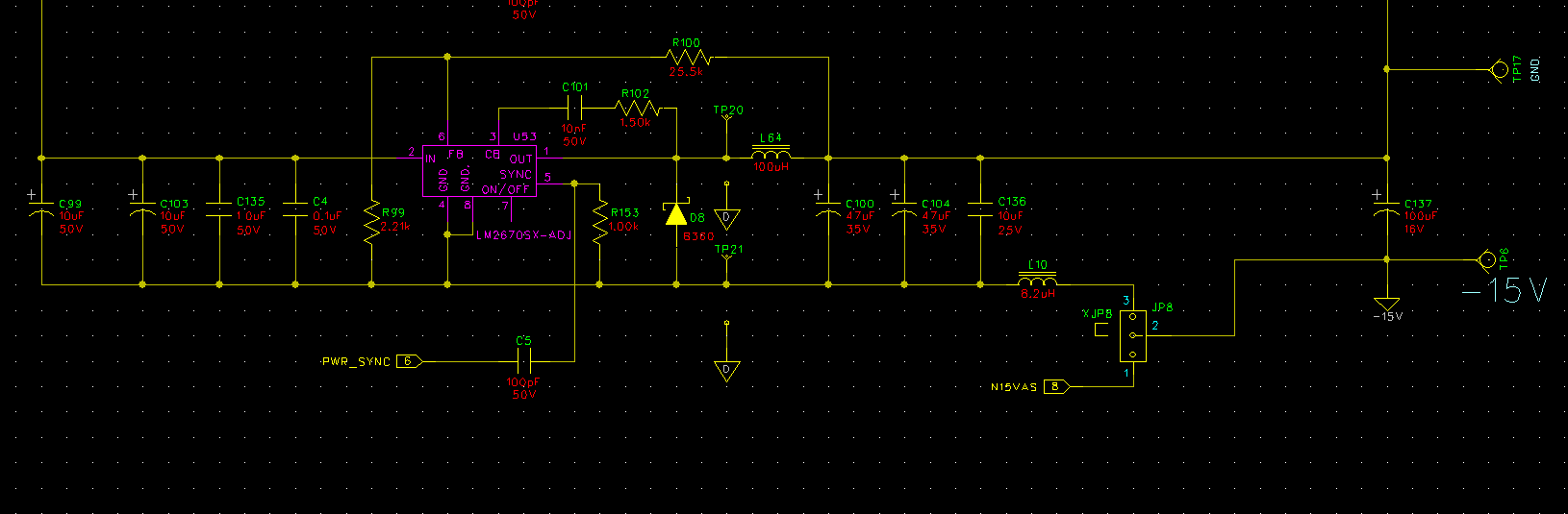
I am using the LM2670X-ADJ IC in a buck boost configuration successfully.  The schematic is attached below for you.  I need to be able to enable and disable this IC.  How can I do this? 

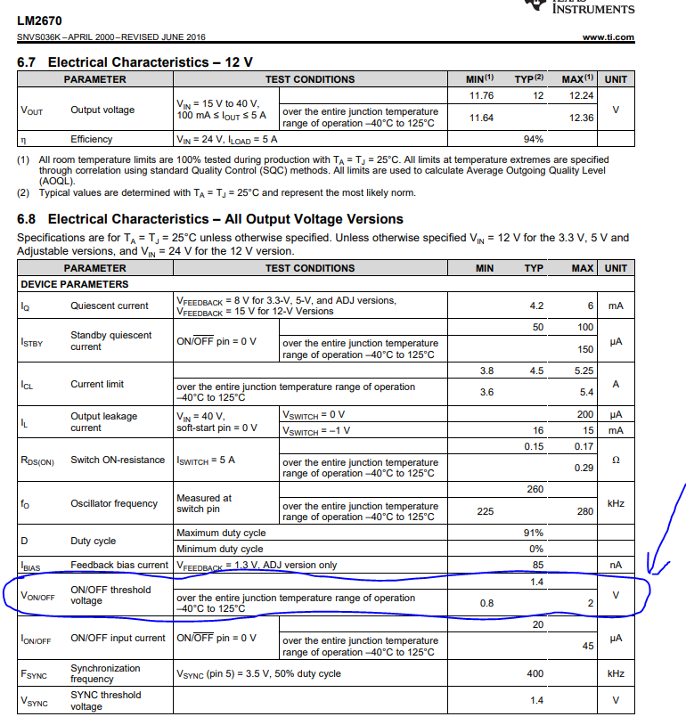
The datasheet excerpt is also given below. It shows that the ON/OFF pin can be set to 0.8V to 2V to turn the device ON.  Likewise a voltage between GND and 0.8V will turn the device OFF.

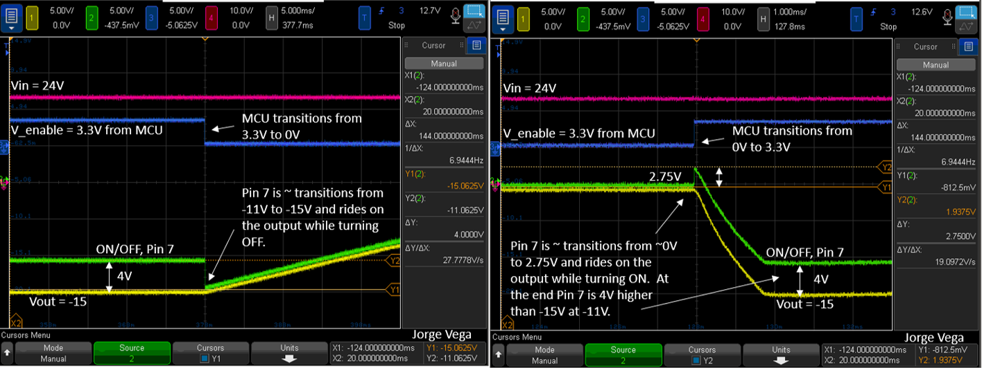
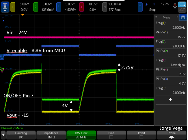
Can you advise what voltages do I need to set the ON/OFF pin to enable or disable my Inverting Buck Boost?  The current implementation has this pin floating (Pin 7).  What levels can I apply to Pin 7 to enable and disable the part?

The section of the D/S is given below:

Many Thanks,

Jorge Vega

  • Hello Jorge,

    I would recommend reading this TI App note to get your issue resolved. Thanks!

    http://www.ti.com/lit/an/snva856/snva856.pdf

    Best Regards,

    Ankit Gupta

    Application Engineer

  • Hello,

    Thanks for the link, its a really good one, but this did not answer my question or solve my problem.

    I need to know what voltage I need to apply on Pin 7 to turn it off.  The topology is a 24V to -15V Inverting Buck Boost.  See the image I posted.

    More background information: I applied -15V with a benchtop power supply to Pin 7 but the chip did not turn OFF.  Is this expected?  

    to recap:

    1. What voltage on pin 7 turns the device OFF given a 24 to -15V IBB  topology?

    2. I applied -15V on pin 7 and expected the device to turn OFF, is this expected? 

    Thanks,

    Jorge

  • Hello Jorge,

    I don't think you apply -15V directly to pin 7 to turn off the device. Because VOUT will go to zero and you still be providing negative voltage to EN pin which can turn on the ESD diode inside the IC. I would highly recommend deploying level shifter circuitry on Pin 7 as mentioned in section 7.2 of the TI App note I referred you before.

    Best Regards,

    Ankit Gupta

    Application Engineer

  • Hi Ankit,

    I was able to use a modified version of the level shifter ckt on Frank De Stasi's app note to successfully enable and disable LM2670 (figure 9). 

    The key to doing this lies in the fact the ON/OFF pin 7 cannot see higher than 6V relative to -15V otherwise the part breaks down when turning ON. This is actually in the D/S page 11 on section 7.3.7. 

    So for this application pin 7 needs to have anywhere from -15 to -14.2 relative to -15 to turn OFF (in other words about 800mV from the most negative voltage).  To turn ON, the device needs to see a voltage between -12V and -9V relative to -15 (6V from the most negative voltage MAX). 

    I worked around these values such that in my application I turn LM2670 OFF when I apply the most negative voltage to pin 7. Conversely to turn the device ON when I apply 2.75V above the most negative voltage. 

    So if the device is ON and regulating, I apply -15V relative to the output which is -15V to turn it OFF.  If wish to turn ON I then apply a divided down voltage that results in about  2.75V relative zero volts to turn it ON (in this case the output of the regulator is OFF and at zero volts), in the end bc I use a divider this voltage grows to 4V which is lower than the 6V limit shown on the D/S.

    The scope shots show the detail while the circuit shows the level shifter I used.  Care needs to be given such that the gate of the FETS can withstand +24V and -15V swings. To this end I chose a PMOS from DIODES INC, DMP510DL-7 that can withstand +/-30V at the gate.  Both FETS need to withstand from 24V to 39V BVDSS.  The FETS I chose have BVDSS rating of 50V PMOS and 60V NMOS.  The Resistor ratio I used is 80K to 10K.

    Cheers, Many thanks,

    Jorge

    The Ckt:

  • Hello Jorge,

    Great news, you could able to get it working. Please let me know if you have more questions. 

    Otherwise, please close the thread if you think your problem is resolved completely. Thanks!

    Best Regards,

    Ankit Gupta

    Application Engineer

  • Hello Ankit,

    Let me ask you about the Sync pin (pin# 5).  Presumably this pin also requires level shifting however I am using a cap to remove the DC and only pass AC to the sync pin.  Do you see any trouble with this?  I loose the sharpness of the corners on the clock, which is 280KHz, do you foresee a problem with this?

    Many thanks,

    Jorge

  • Hello Jorge,

    You must use level shifting circuitry for sync in Inverting Buck-Boost Application. IC performs much more reliably and would have no problem detecting low level and high level of sync pin. Hope this helps!

    Please close the thread if you think your problem is resolved completely. Thanks!

    Best Regards,

    Ankit Gupta

  • Thanks for your help.  This resolves my issue.  Thanks again.