This thread has been locked.

If you have a related question, please click the "Ask a related question" button in the top right corner. The newly created question will be automatically linked to this question.

BQ25120A: Reg. the official Dev Kit Schematics

Part Number: BQ25120A

Hello,

I have some queries related to the hardware schematics and programming of the BQ25120A IC and will be grateful for your responses:

1. Do I have to permanently keep the host connected to the BQ25120A? Or can I program the BQ through the HOST and remove it?

My query basically comes from a situation where if the battery completely drains and remains drained for many days, then the BQ may not even receive a quiescent current in which case, it may lose all its firmware that I have programmed. Please explain this.

2. My system comprises a microcontroller and 2 sensors. The system requirements are regulated 1.8V, instantaneous current of 250 mA and average/ continuous current of 25-30 mA. Can I simple make a power rail from the SYS and GND pin or should i attach my microcontroller to the SYS and GND pins and the 2 sensors on the LS/LDO pins?

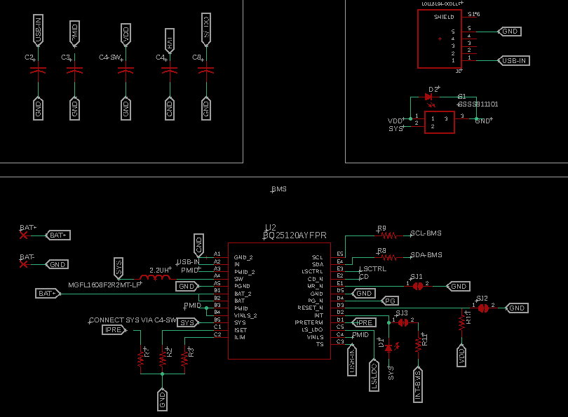
3. I want to add an LED to indicate the charging status (when my battery is charging through USB charger). In the schematic attached below, I have put an LED between SYS and INT, with hope that when charging, INT will go LOW and SYS will be at 1.8V (which I will program through HOST). Is this correct?

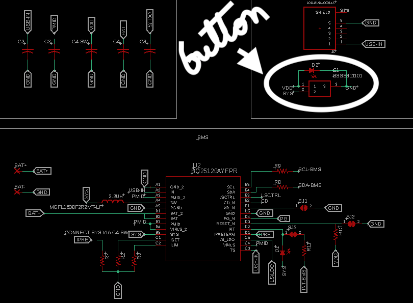
4. I also want to put a button between my Battery Management System and my system (Microcontroller + 2 Sensors). I plan to put this at the SYS output, in the way shown in the schematic. Am I correct in doing so?

PS: VDD is supposed to be the regulated 1.8V in my schematic. SSSS11101 is a slider switch (On/ OFF). Rest all labels are as per the datasheet and the official dev kit schematic itself.

Any help, corrections will be highly appreciated!

  • Hello Anmol,

    1. The BQ25120A has a 50s watchdog timer which needs to be serviced by the host to prevent the registers from reset. However, if you pull /CD low when in battery only mode, the device will be in a low Iq Hi-z mode which disabled the watchdog timer.

    2. You want to power the MCU from the SYS pin to ensure the all the voltage rails are the same especially IO pins. The sensors can be connected to the LDO since this will give you the option to turn off the LDO and power to the sensors when not needed which can reduce your system Iq.

    3. Yes. You want to enable the EN_INT bit which is B3 in 0x02h. I'll suggest adding a resistor in series with the LED.

    4. I don't see this button in the schematic. Can you please pont this out. Also what is the reason for adding this button.

  • Hello Raheem,

    Thank you so much for the response and so sorry for the delay in mine.

    1. Would it be enough to then keep CD, SCL, SDA & INT connected to the host at all times, but eliminate the necessity of keeping LSCTRL & MR connected forever? I am desparate to reduce the number of wires in the final design.

    2. The recommendation is very helpful, thank you!

    3. That was a rookee mistake about the resistor before the LED, I am embarrassed! But does the INT pin not automatically pull low when charging? It says so in the data sheet! OR do I have to code the chip to enable the INT and pull it to LOW every time the charger is sensed?

    4. The button is right here, in the image circled below!

  • Hello,

    1. Yes, you want to connect SCL, SDA, /CD and /INT to the host at all times. The LDO can be controlled in the register settings but you need to have LSCTRL pin pulled high to do this. /MR is a pushbutton input so you only need a pushbutton on the pin.

    3. /INT is open drain. The charge status is shown by default.You dont need to make any register changes.

    4. I don't see any problems with the button/switch between SYS and your system.