Hello:
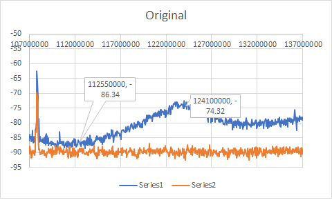
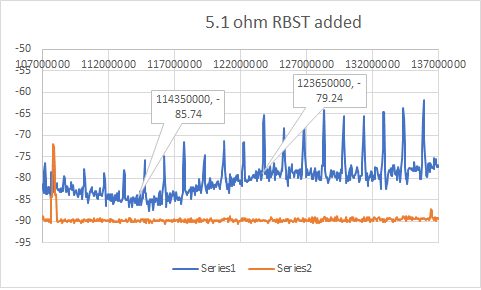
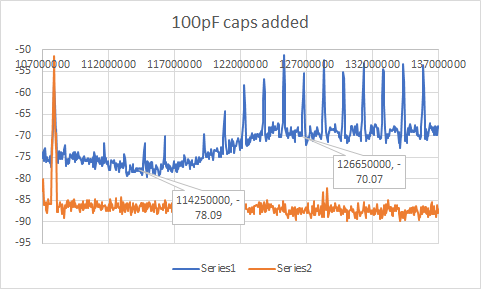
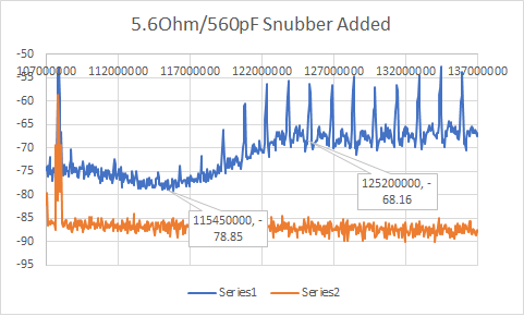
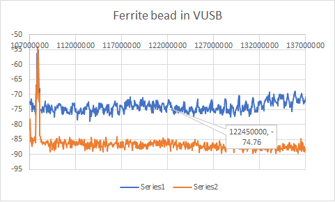
We have a product using the BQ25886 that underwent FCC pre-cert and failed on a frequency band near 120 MHz. The noise profile is similar to noise that a boost generator generates and we have isolated the problem to our on-board BQ25886 in the testlab as well as in our lab. The noise completely disappears when the USB charging source is removed. We have used the USB charging source in other devices that have passed FCC, so we eliminated the charger as the issue. I suspect the noise is originating from the SW node - we have nothing else on the board that switches quickly.
I would like to ask TI to review our waveforms and schematics with us, but I cannot post these on a public forum. Is it possible to get a private channel to talk through for this?
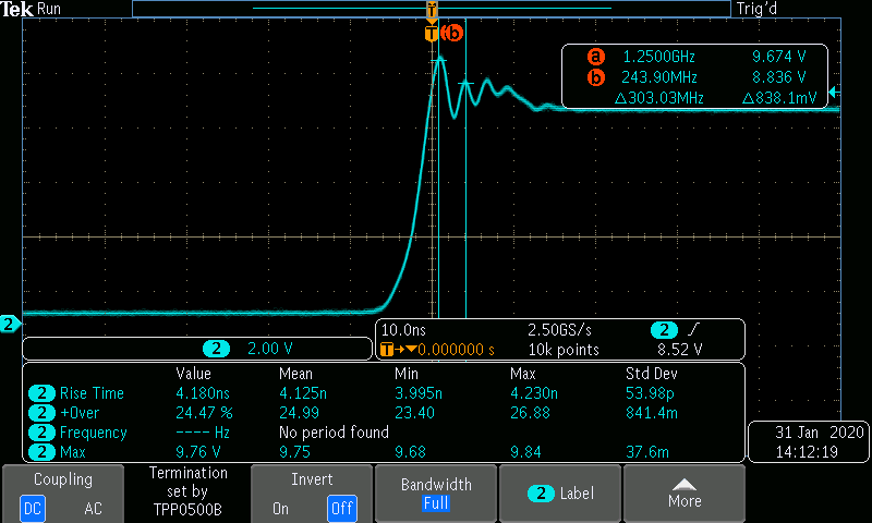
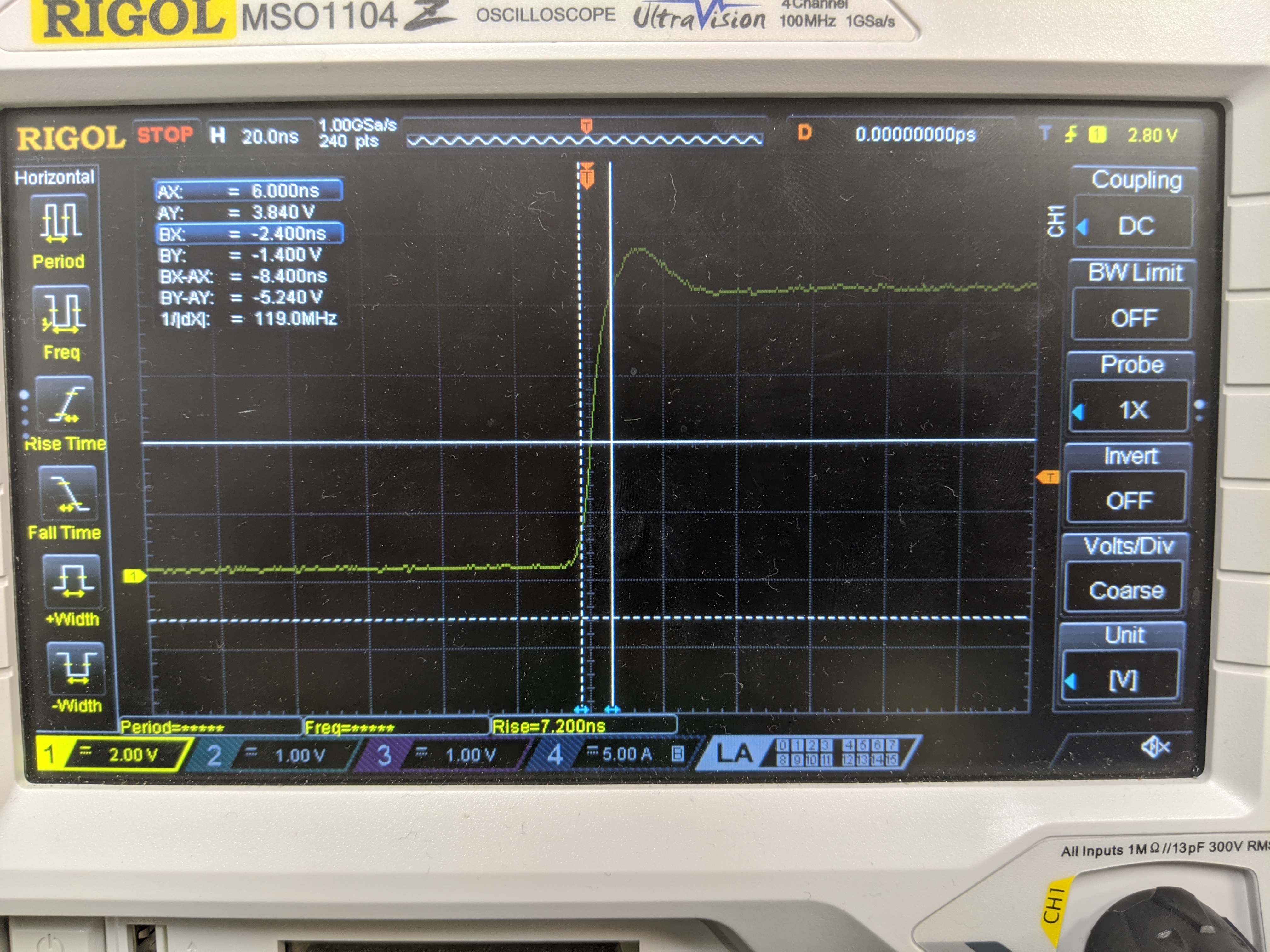
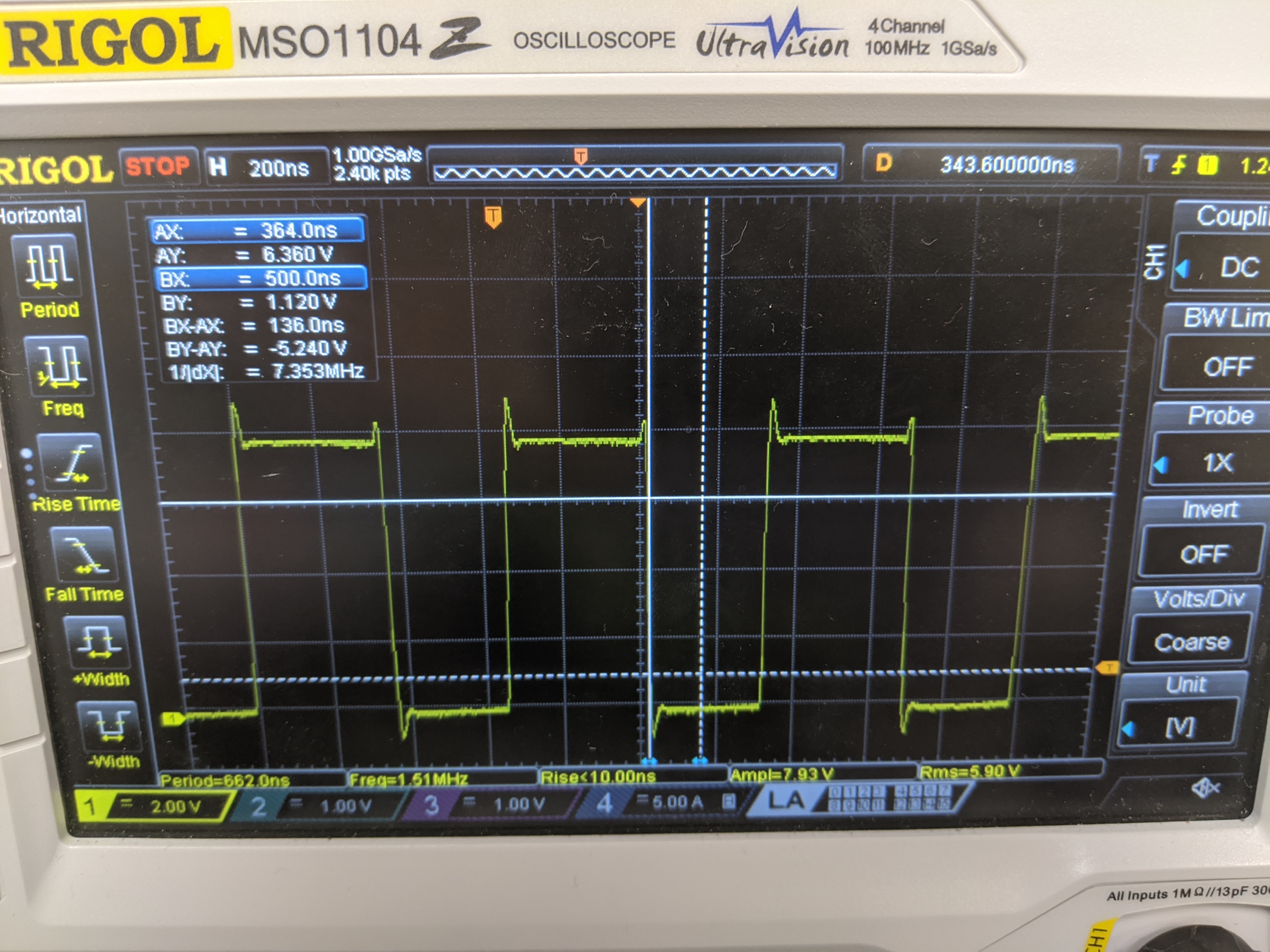
Also, I checked the SW pin for ringing, but I really cannot see any significant ringing on the pin. However, every time I touch the pin it seems to make the problem worse. Here is a picture of the scope of pin SW (sorry, USB port is acting up!). I have tried to calculate the RC for a snubber following SLVA790a, but it does not seem to affect the overshoot (tried from 1pF to 47pF and no noticeable difference on frequency, which is the first step of that document).
Pictures of SW pin in mode that fails FCC.
Thank you!