This thread has been locked.

If you have a related question, please click the "Ask a related question" button in the top right corner. The newly created question will be automatically linked to this question.

BQ25713: High current VSYS application

Part Number: BQ25713

Hi there,

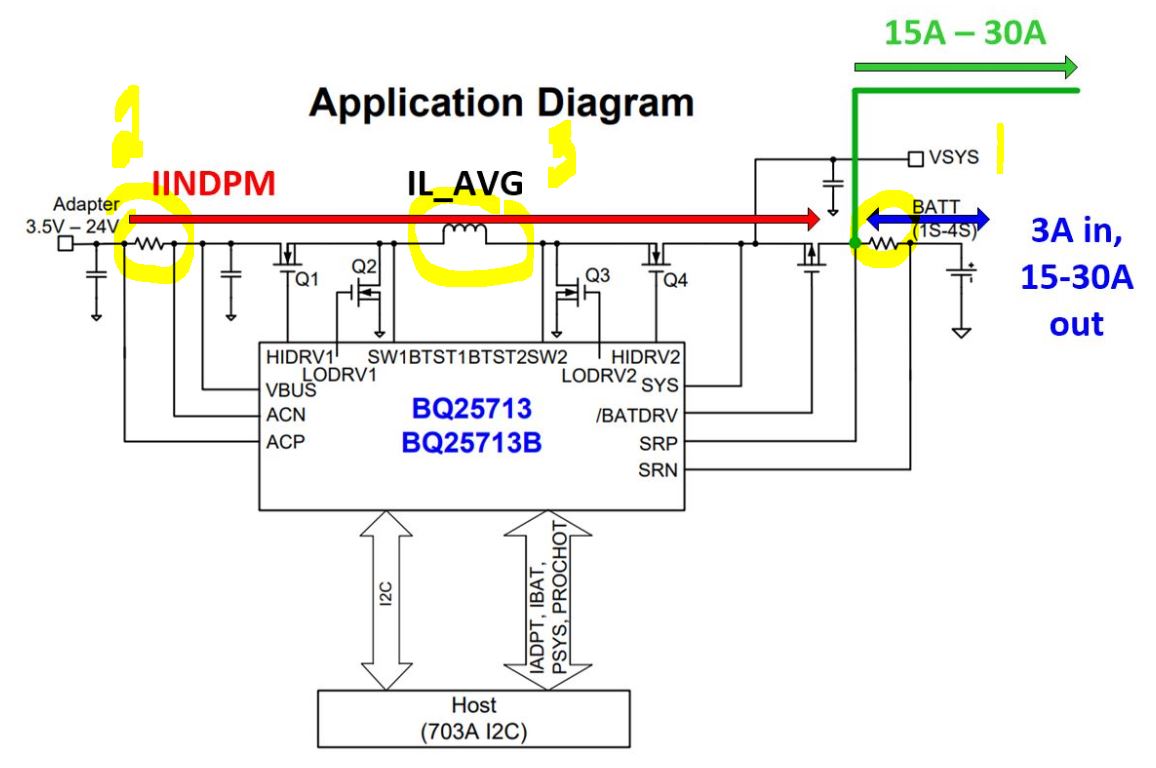
I'm planning on using the BQ25713 as a buck/boost battery charger for high capacity 3S lithium battery with around 90Whr capacity, typically operating with 12-20V charger input at 3A. The system requires high peak currents in the region 15-30A from the battery. This seems too much to follow the standard configuration in the EVM and reference designs - it's not really possible for me to run these high currents through a 10mOhm resistor and BATDRV p-channel MOSFET. 

So I assume I just leave out the BATDRV MOSFET and then connect my system directly to the battery? The BQ25713 will still monitor the current flowing out into the battery but will not be able to monitor the current drawn by the system. 

Are there any reference designs for this sort of application? How does the schematic differ? 

Any help and advice would be appreciated. 

- David

  • Hey David,

    Normally, I would recommend you move to using a 5mOhm RSR (I found some 5W and 10W ones on Mouser) so your peak power loss through the resistor is 4.5W. 

    In this scenario, you can still use the discharge ADC measurement of the battery current, but you will have to scale the ADC values from the datasheet as it assumes a 10mOhm resistor. The same goes for the charging current setting values. 

    Because of your scenario, you will likely need to forgo using the SYS node as your system rail, and instead tie directly to the battery as you mentioned. This means your system rail relies solely on the battery voltage, so if your system UVLO > battery depleted voltage, you will have a scenario where the system will brown out. 

    If you want to remove the BATFET, you need to follow paragraph 3 of section 9.6.5.1 System Voltage Regulation in the datasheet. One caveat that is not listed in this section (although to be added in a revision to the D/S) is disabling charge. When the charger is operating without the BATFET, you can only disable charge by placing the converter in HIZ mode. 

    Now to use the discharge ADC reading, you would actually connect your system load to the SRP node instead of the SRN node, such that discharge current still flows through the RSR resistor. 

    And as a last comment concerns the slew rate of your 15-30A system load. If the slew rate is <50us, I would suggest utilizing the IL_AVG bits which program the cycle-by-cycle peak inductor current. By default, this value is 15A. For loads faster that 50us, the converter in this configuration will attempt to the provide the full 15-30A until the cycle-by-cylce current limit is reached. At slower loads, the IINDPM loop will kick in and forcibly limit the input power to VBUS x IIN_HOST setting. 

    Regards,

    Joel H

  • Thank you for the reply. 

    The application means that the system will run from the battery "most" of the time with charging happening periodically. I worry that having a p-channel mosfet in the way will cause me problems. 

    It seems I could either try using a high current p-mos (<5mohm Rdson) and lower the RSR to 5mohm as you suggested, or connect the system directly to the battery. 

    Either way, I will keep the BATFET it seems as this is the way to disable charging. Perhaps I'll allow myself to select where the system connects in my first design so I can try using the RSR and BATFET first. 

    I don't really understand your comments on the slew rate - can you explain? I've only been working with this IC for a few hours so not really fully up to speed on it yet. 

    Are there any limitations on the RSR ADC current readings? Apart from correctly rating the resistor. 

    Thanks again

    David

  • Hey David,

    You can certainly leave the BATFET populated, and the converter will provide most of the current through the BATFET. 

    Using the figure below, I can clarify some things, and reference some of the highlighted points:

    The Red current path is the power coming from the converter from the input through the converter. 

    The Blue current path is the battery current (either charging or discharging).

    The Green current path is the system load discharge path. This is where you would connect your system.

    While charging, the converter is trying to regulate area (1) to give you 3A of current. However, due to the system load connection, the 3A would be diverted to the system rather than the battery.

    This is where area (2) comes in at the input. In the scenario above, the converter will continue to output current until it can provide 3A through area (1). If the system load is very high at that point, most likely the charger will hit the IINDPM threshold which is monitored and regulated through the area (2). This is an input current regulation loop which regulates the DC input power. 

    However, because it is a regulation loop intended more for DC current regulation, my previous post comment about the load slew rate applies. Here, we focus on section (3) and the IL_AVG register setting. This control can take over in the time between a fast/large load step and the IINDPM regulation loop responding in order to regulate the peak inductor current. 

    Regards,

    Joel H

  • Hi Joel

    Thank you for clarifying. Did I mention that it's an audio application?, so the VSYS current will follow an audio signal and have high fast transient peaks and generally be of AC nature. Therefore I think it's going to be best to run the VSYS directly from the battery.  There's no way I would get any meaningful reading from the current sensor so there seems little point in doing so. Also, the charger might have trouble regulating the current. 

    How about I run all the constant quiescent loads through the current sense resistor and connect the speaker amplifier directly to the battery? At least this way I can monitor most of the load? 

    I still don't understand the point in connecting VSYS to the left of the PMOSFET as opposed to the right as you have drawn it in green... perhaps you could explain the purpose to me?

    Thank you for your help

    David

  • Hey David,

    That is fine by me. This was to allow you to monitor the discharge current.

    David Trotter said:
    I still don't understand the point in connecting VSYS to the left of the PMOSFET as opposed to the right as you have drawn it in green... perhaps you could explain the purpose to me?

    I am still connecting this to the right side of the PMOS; I'm just connecting to the left side of the sense resistor. This was only to allow you to utilize either the internal ADC or the IBAT pin to monitor the discharge current.

    Regards,

    Joel H