Other Parts Discussed in Thread: LM5050-1
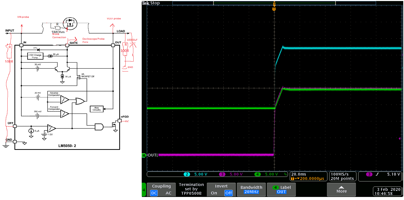
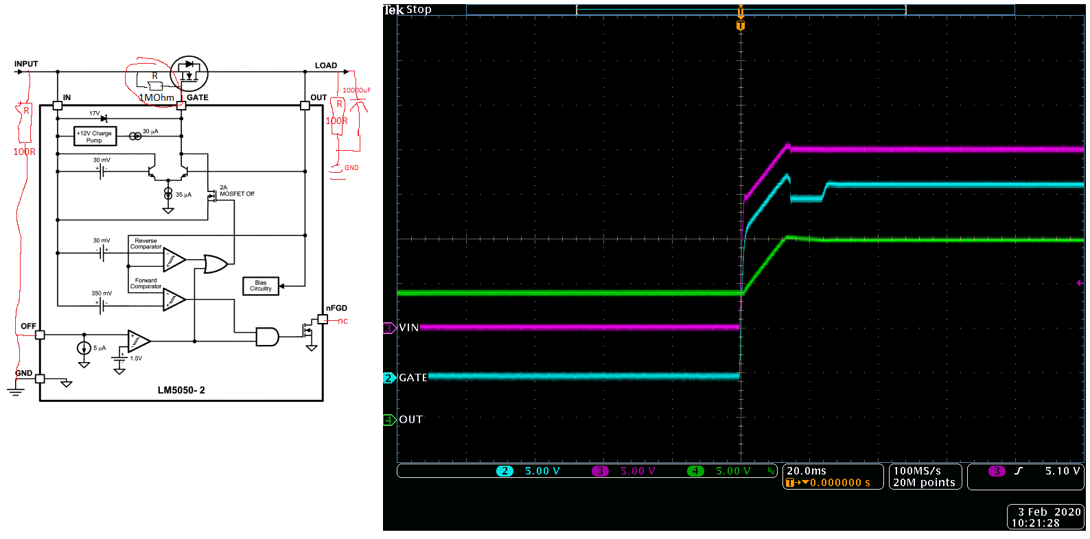
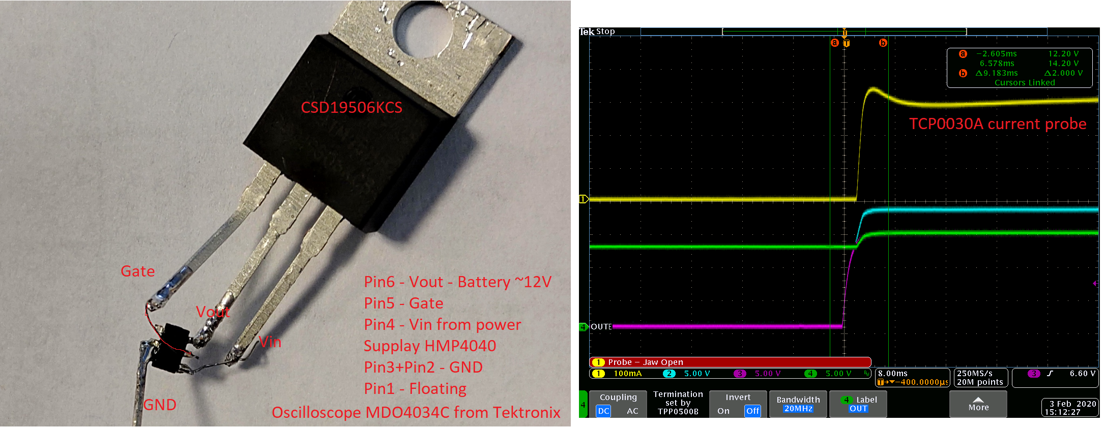
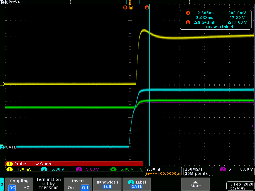
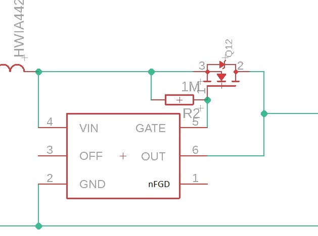
Schematic is look like this: Q12 is CSD19506 or CSD19505
Gate Charge Total (10 V) 120nC
Gate Charge Gate to Drain 20 nC
Drain-to-Source On Resistance VGS = 10 V 2.0 mΩ
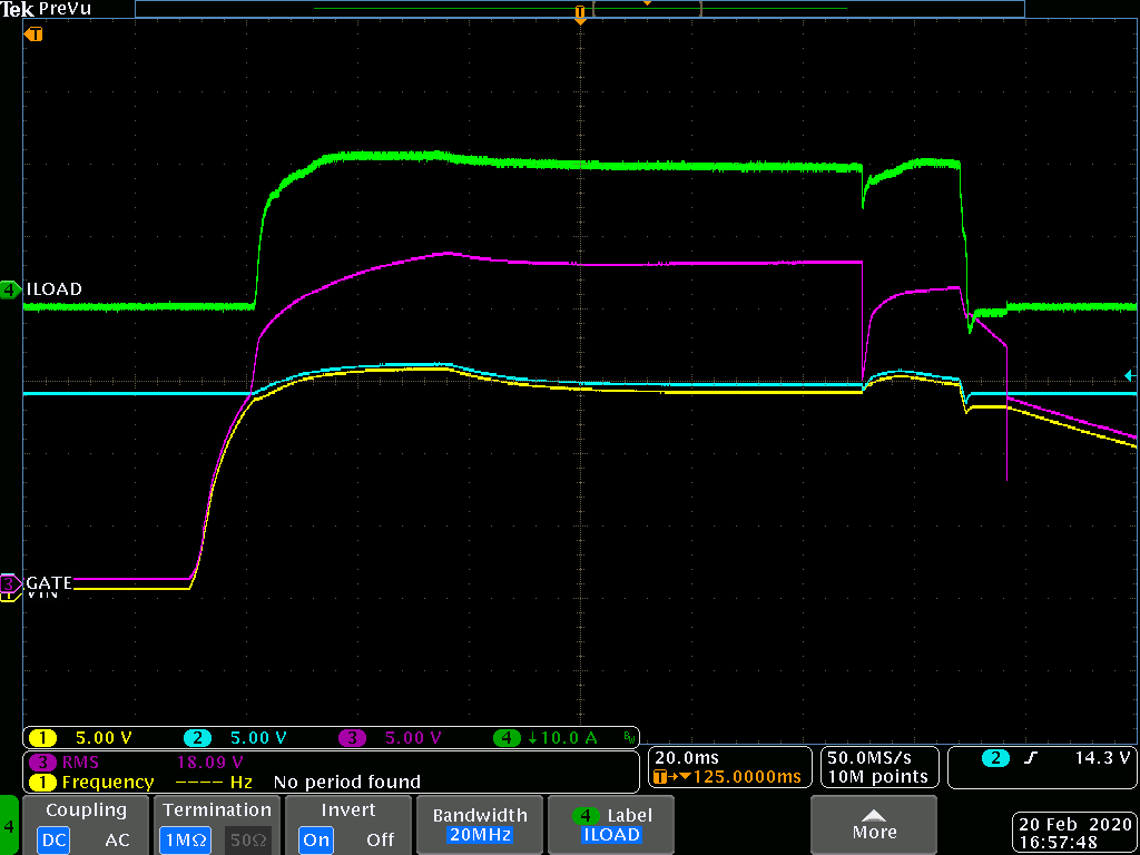
Offset is ~4-5 V above Vin.
2 test:. I removed pool-down resistor to verify if have some changes. The same issue.
3 Test. I add a 100Ohm from gate of lm5050 to gate of Mossfet. The same result.
4. I cut line between gate of lm5050 and Gate of mossfet. Here I have 14-16V Offset.
I tried with 2 chips. Thes same results.
On monday I can provide picture from oscilloscope to confirm my investigation.
please give me any suggestion.
thanks.