This thread has been locked.

If you have a related question, please click the "Ask a related question" button in the top right corner. The newly created question will be automatically linked to this question.

LMG1205: LMG1205 phenomenon that looks like latch-up

Part Number: LMG1205

We are using the LMG1205 bootstrap gate-driver for driving EPC2020 GaN transistors, and we seem to be facing what looks like a ‘latch-up’ issue, resulting in our GaN transistors blowing up. We suspect that this is related to the high oscillations during soft-switching transition, at high currents. However, to come up with preventive measures, we are trying to understand what part of the LMG1205 IC is malfunctioning, and what exactly is the trigger for this latch-up-like action. 

Circuit Description

For the half bridge structure, both the high-side and low-side switches are comprised of three parallel EPC2020 transistors. Our application involves peak currents of over 200 A through the combination of three parallel transistors; the RMS currents are lower (max 100 A). Thus, at the instant of switching, the switching current can be as high 200 A. To assess the switching performance, we have performed double-pulse test for the half-bridge. While the hard-switching transitions are fairly satisfactory, the oscillations during the soft-switching transitions are much worse.

So far, we have attempted DPT at >170 A three times, with varying values of external gate turn-on resistance (10 ohm to 18 ohm), turn-off gate resistance (1 ohm to 5 ohm), and varying values of snubber capacitance (0 nF to 15 nF, per switch). On all three DPT attempts, we have encountered a failure caused on exactly one of the three paralleled transistors on the high-side. The specific transistor that fails (based on location on the PCB) has varied; however, the failure always occurs on a high-side transistor. Attached please find a schematic of the circuit being tested.


Problem Description

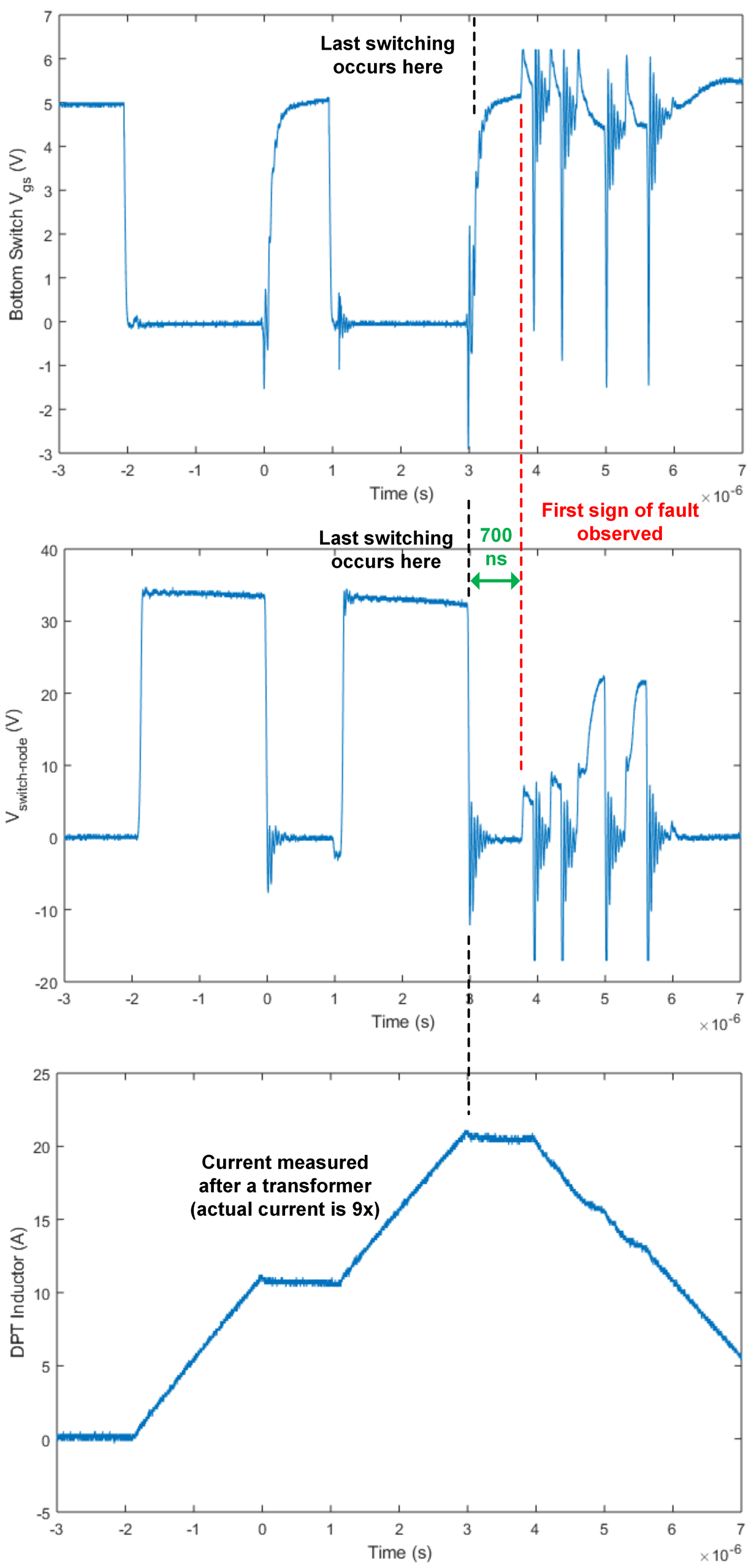
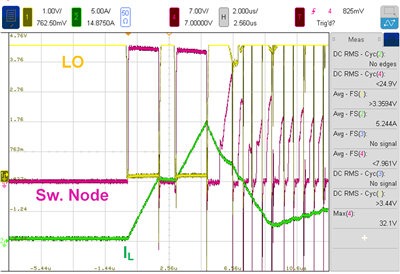
During the soft-switching transition, we found that the switch-node voltage (i.e. the voltage between HS and VSS) is having a high negative overshoot. For the circuit operation with 15 nF added snubber capacitor per switch, Rg,on = 18 Ω, Rg,off = 5 Ω, the switching node voltage seems to go below -10 for 15 ns, as measured close to the gate driver pins, as shown below in the extracted experimental data from one of the failure instants. Due to limitation of available probes and test points, the gate voltages are measured using the Keysight N2894 700 MHz non-isolated probe with pig-tail ground return, the switch-node voltage is measured using a Keysight N2790A 100 MHz differential probe. The inductor current was measured using a N7026A 150 MHz probe connected after a current transformer.  


Interestingly, rhe first noticeable symptom of the fault occurs nearly 700 ns after the switching transition. Subsequently, the switch node voltage shows a periodic rise (even when the bottom switch gate is held high), and hence we are suspecting that LMG1205 is going into some sort of a latch-up mode. It appears that the top switch starts conducting while the bottom switch is still in ON condition, causing what appears to be a short circuit current to flow, and thus developing a voltage at switching node (Ids* Rds,on). 

Hence, we are trying to find answers to the following questions:

(a) We could not find any details on latch-up response of LMG1205 - how does it respond to negative voltages on the Vs pin - will it pull up both high-side and low-side gate outputs to 5 V?

(b) How does LMG1205 typically respond to the negative voltage between HS and VSS pin? Could LMG1205 latch-up in this scenario?

(c) Apart from the negative voltage on HS pin, is there any other condition (undesirable voltage on some other pin) that could cause the issue that we are encountering?

(d) If this is indeed a latch-up problem, what measures could we take to avoid this phenomenon?


  • Hi Akshay,

    thanks for reaching out on e2e on Lmg1205.

    Thanks for explaining your issue. So the failure happens to the high side FETs only?

    Can you take a waveform of multiple waveforms on the same plot?

    if so, can you capture HO, LO and the switchnode on one plot?

    also, can you take another waveform of HB-HS so we can see if the negative HS voltage is overcharging the bootstrap (when the issue happens).

    HB-HS should always stay at 5V. so that HO can stay under the 6V GaN gate max.

    I dont see the 18 and 5 ohm resistors, are they on the schematic you share? are these gate resistors or snubber resistors?

    can you share your gate drive portion of the layout with me?

    its possible the high switchnode current is affecting the gate loop from the FETs common source inductance introduced by pcb layout inductance.

    Thanks,

  • Hi Jeff,

    Thanks for looking into this.

    It took us a while to rework the board after the preceding failure, mentioned in the original post. Please find below the responses to the questions you asked, along with the relevant waveforms. While the waveform in the original post corresponded to the instant of switch blowing up (at 35 V, 190 A), this time we have lowered the DPT voltage/current to (23 V, 128 A) to prevent the switch from blowing up during the process of capturing all the different waveforms.

    1. Yes, we have seen the failure consistently happen only on high-side FETs (3 times of 3, so far).
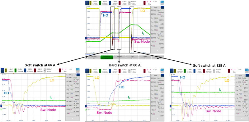
    2. HO, LO and switch node on one plot. Due to instrumentation limitations, HO is measured is using a Keysight N2792A differential probe, LO is measured using Keysight N2894A non-isolated probe, and switch node is measured using N2790A differential probe. Looking at HO specifically, we do not see much in terms of noise (dv/dt or di/dt related).

    Fig. 1. HO (yellow), LO (blue), switch node (magenta), and inductor current (green) waveforms (switch node captured across the IC terminals) (23 V, 128 A)

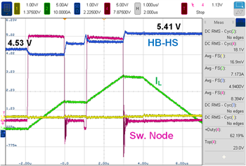
    3. The HB-HS waveform is attached below. While we do see overcharging on the bootstrap capacitor, it is not seen to cross 5.5 V, until up to 128 A tested here. Moreover, after the bootstrap capacitor charges to its highest value of 5.41 V, the HO output should stay pulled to low.

    Fig. 2. HB-HS waveform (blue) (23 V, 128 A)

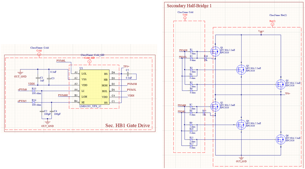
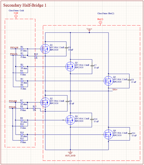
    4. Apologies for the confusing schematic included with the original post. The schematic of the modified half-bridge setup is attached below, with the correct gate drive resistors. Additionally, the snubber capacitors are also shown in this schematic version, which have actually been added to the circuit externally (i.e. not a part of the PCB layout)

    Fig. 3. Corrected schematic for the power circuit part (gate drive IC schematic is as mentioned in the original post)

    Lastly, I have also attached the waveform from my original post in a single oscilloscope screen plot.

    Fig. 4. Oscilloscope screen capture of the waveform included in the original post, at the instant of switch failure (35 V, 190 A)

    We unfortunately have some restrictions in terms of sharing the layout.

    Based on the HO and LO waveforms, we do not see the voltages exceeding the switch or gate drive maximum limits yet. However, the switch node voltage measured near the gate drive IC (magenta waveform, HS-VSS) seems to be crossing the “-5 V” absolute maximum rating for the HS-VSS potential, as specified in the LMG1205 IC. From the collected data, our first guess is that this could be the cause of failure; however, we lack an understanding of whether the Fig. 4 indeed represents a latch-up for LMG1205, and why the shoot-through (which seems to be the cause of failure) gets triggered.

    Thanks!

    Akshay

  • Thanks for the update Akshay,

    Since the high side switch is damaged and from your fig4 waveforms it looks like the high side gate is turning on when LO turns on.

    This seems like an issue where the switch node is going to ground with LO too fast.  The high dv/dt on the switch node can turn the other fet on by capacitive coupling.

    Does the issue still happen with the extra C6,7,8 15nF high side drain to source caps removed ?

    Does the issue get better by increasing R7,9,11 from 10ohm to 20?

    Can you share gate drive portion of layout on e2e private message?

    Thanks,

  • Hi Jeff,

    Yes, we suspect that the high-side gate is indeed turning on when the LO is on.

    However, we cannot explain as to why it happens ~700 ns after the LO crosses the threshold voltage (this delay has been consistent over the three times that we have encountered this), for the switch node to show any meaningful increase in voltage (ref. Fig. 4 from my previous post). Moreover, this pattern then keeps on repeating periodically a few more times before the circuit (apparently) stops functioning and everything goes quiet. The 700 ns delay, and the repetitive nature of the fault made us guess that it could be some unique way that the gate drive IC is responding.

    While the di/dt rates are very high, the dv/dt rates in the circuit are rather low (<5 V/ns). LMG 1205 datasheet mentions a HS slew rate of 50 V/ns. Could the dv/dt still be an issue?

    About the C6, C7, C8 snubber capacitors – in fact our original circuit did not have these, as we did not anticipate the need for added snubber capacitors. The first time we experienced a switch blow up, these capacitors were not present. Attached below is the screen freeze of this aforementioned first blow-up during DPT (distinct from Fig. 4 from my previous post). In the figure below, we did not position the LO signal properly on the screen, hence it is seen as clipped. The basic failure mechanism seems to be identical, however the repetitive pulses were more in number before things went quiet. Additionally, this failure occurred at 179 A (slightly lower than the 190 A for Fig. 4 in my earlier post) - the key changes between the two tests were that the 190 A failure occurred with the snubber capacitors present, and higher values of turn-on and turn-off gate resistors respectively (while the 179 A failure in Fig. 5 below had no snubber capacitors, and lower values of R_g,on and R_g,off) .

    Fig. 5. Failure waveform without capacitors (C6, C7, C8)

    About increasing R7,R9,R11 - from 10 ohms to 18 ohms, and we saw a small improvement, in terms of the ZVS transition at the maximum current. We found that increasing R8,R10,R12,R2,R4,R6 had a relatively more significant impact (in terms of the ZVS transition becoming slower, hence lower undershoot), but still a somewhat small impact overall.

    I have shared the layout with you in a private message.

    Thanks!

    Akshay

  • Thanks for the update Akshay,

    Thanks for trying out the circuit mod.

    If slowing down the switching with a higher gate resistor value does not significantly help the issue it's possible our problem lies with GaN and driver layout. Since this is DPT there is very high current and it's possible that the high di/dt in the power loop is causing the gate to lift wrt the source. Even though the dv/dt is slow the common source layout inductance is too much for the high di/dt. Since the lift the gate can see is proportional to the amount of common source inductance as well as the di/dt.

    Let me review your layout and continue our thread on private message.

    Thanks,