This thread has been locked.

If you have a related question, please click the "Ask a related question" button in the top right corner. The newly created question will be automatically linked to this question.

TPS62130A: Output Ringing at Light Load

Part Number: TPS62130A

Hi TI team,

I meet an issue when using TPS62130A as power supply IC to supply 3V8 for main power VBAT of MCU SC20 Module from Quectel.

To describe my issue, I will you the information:

  • MCU SC20 Module recommended input voltage range: from 3.5V to 4.2V
  • Schematic and Layout Design: the same as ref design of TPS62130A datasheet
  • Input Voltage: 5V @ 5A max
  • Output Voltage: 4.01V
  • Switching Frequency: Connected to GND => fsw = 2.5MHz
  • DEF pin: Connected to GND => Nominal scaling output voltage.

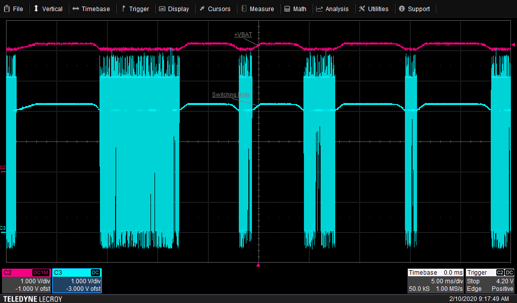
When I plugging in power supply, output voltage VBAT rises normally and SC20 starts to boot up.

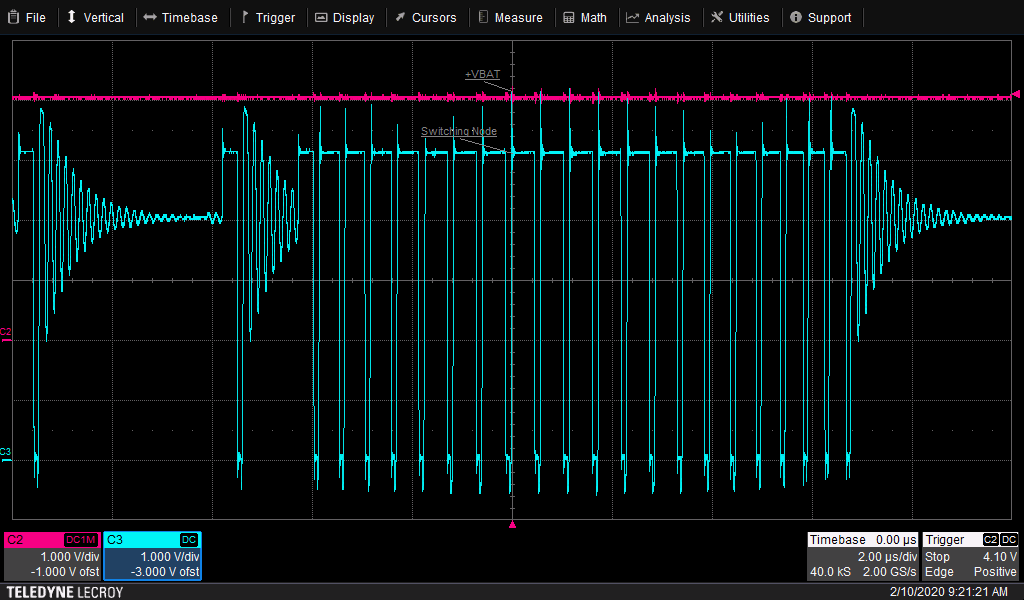
After about 40s, SC20 completely boots up, VBAT current decreases to less than 50mA, then ringing issue happen as above picture.

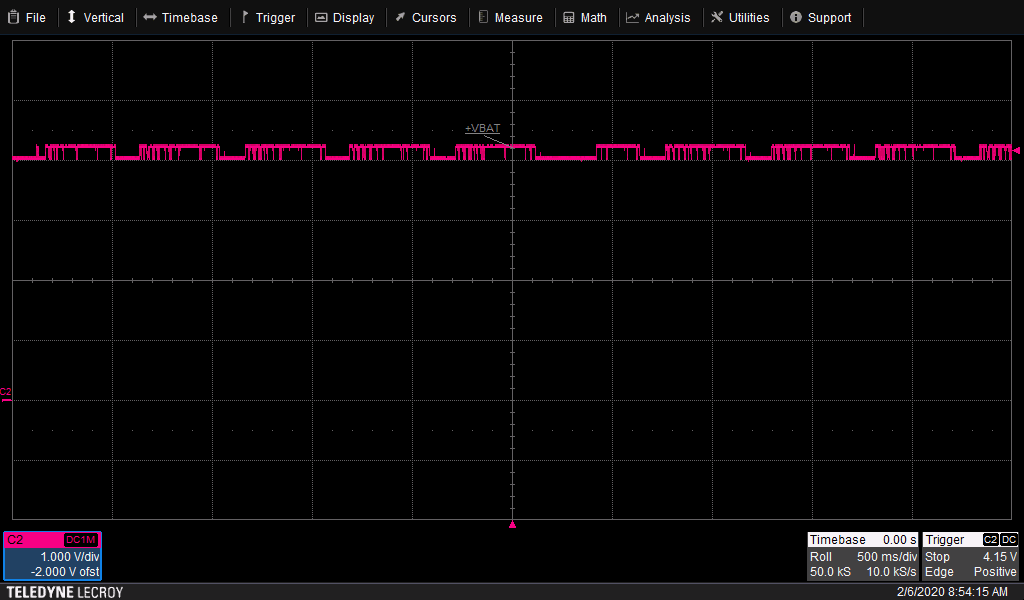
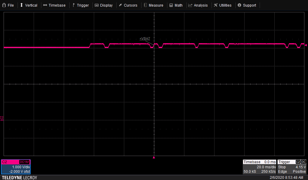
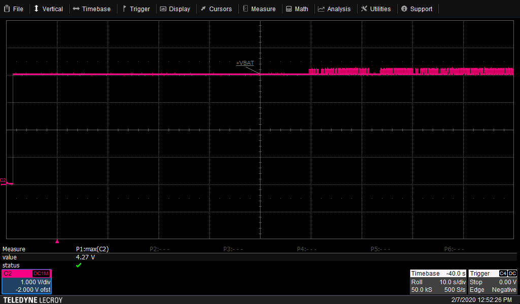
Can see that, the ringing looks like malfunction and Peak Voltage is 4.27V which will be risk to the MCU.

As I read on the datasheet, TPS62130A has internal DCS-Control so that the transition from PWM mode to Power Save Mode is seamless without effects on the output voltage. Unfortunately, at Light Load < 50mA, this ringing happens to my design.

I isolate TPS62130A module and test with simulation constant load, it works normally.

Please give me your feedback about this issue.

Trong

  • Trong,

    Actually, the load regulation may vary by about 30 mV between light load and PWM operation as shown in the datasheet Figure 22.  However your case is more like 200 mV, which is abnormal.  Did you follow the datasheet layout guidelines precisely?  In the mean time I would like to see more waveforms.  Pleas zoom in and trigger on the rising edge of the VOUT voltage increase.  To start with let me see VOUT, the SW node voltage and the load current.  Do the same on the falling edge.  Try 2 usec / div and 10 usec / div.  Increase the time scale further if needed to get a clear picture.

  • Hi John,

    I have re-checked my layout design and confirm that it follows the layout guidelines in datasheet.

    Here is some waveforms as your request:

    Measurement point:

    Zoom out:

    Zoom In:

    After observing these waveforms, I see that:

    1. Switching node does not work when +VBAT peak to 4V2

    2. As I shorted Pin 7 - FSW to GND, the switching frequency is about 1.5MHz, not 2.5MHz as desired.

    3. Transition between PWM mode and PSM mode is fine, happen when +VBAT normally at 4V.

    I do not have current probe so that I can not show you load current waveform, I detect my issue happen at light load <50mA by using VOM in series to measure +VBAT current.

    Please give me your ideas and feel free to ask if you need more information.

    Trong.

  • Trong,

    This looks like a simple case of loss in your circuit.  In the places where Vout is higher there is no switching because the load is light or no load.  There are no losses as there is no current draw and the output voltage is higher.  When the load is applied, the device starts switching.  The loss in your PCB layout is likely causing I*R voltage drop.  Let me know if you can upload the PCB layout.

  • I will go ahead and close this thread for now.  You may re-open it any time.