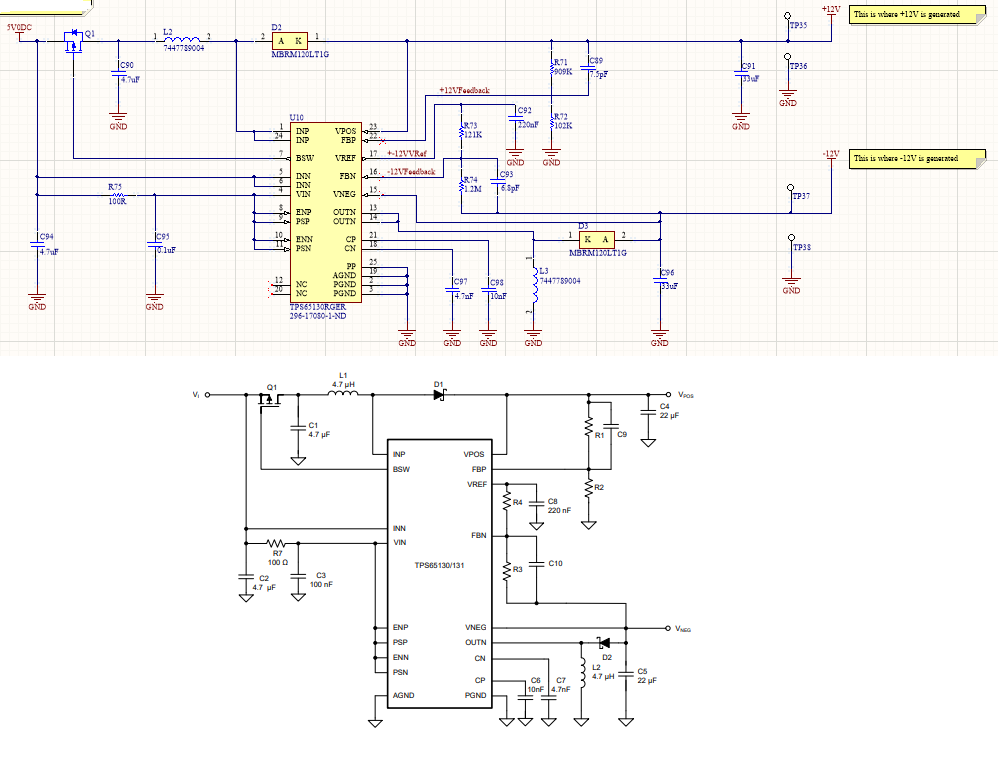
I tried to follow the data sheet and create a circuit based on the TPS65130.
I wanted two rails +12V and -12V from a 5.0V supply.
My schematic (witch matches data sheet - also included in photo at bottom) is :
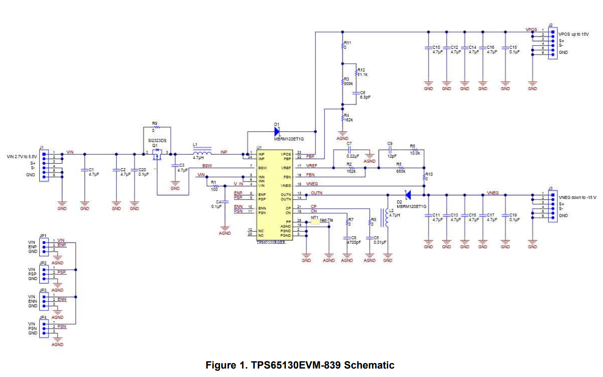
From the EVM:
The schematic from the EVM:
1) ENP/PSP/ENN/PSN are all directly connected to Vin signal in the EVM (not the VIN pin). In the data sheet they are after the 100 ohm resistor and tied to the VIN pin. which is correct?
2) The negative feedback in the EVM has an extra 10K resistor (R5) that is not shown in the reference design (No resistor in series with C10, parallel to R3).
I currently get < 1.0V on +12V rail and 0.4V on -12V rail.
My layout follows very closely the layout for the EVM, minus the schematic differences noted above in 1) and 2).


