This thread has been locked.

If you have a related question, please click the "Ask a related question" button in the top right corner. The newly created question will be automatically linked to this question.

TPS7A03: Regarding Active Discharge

Part Number: TPS7A03
Other Parts Discussed in Thread: TPS797

TPS7A03, as well as several similar devices, has active discharge. It is not a feature we see we need or benefit from in our setup, but TPS7A03 appears to be a suitable device in general. Reading about the active discharge in the datasheet we have two questions:

1. It is stated that active discharge is limited to the P-version. We cannot see that there is any other version listed, such as TPS7A0333DQN. Is there?

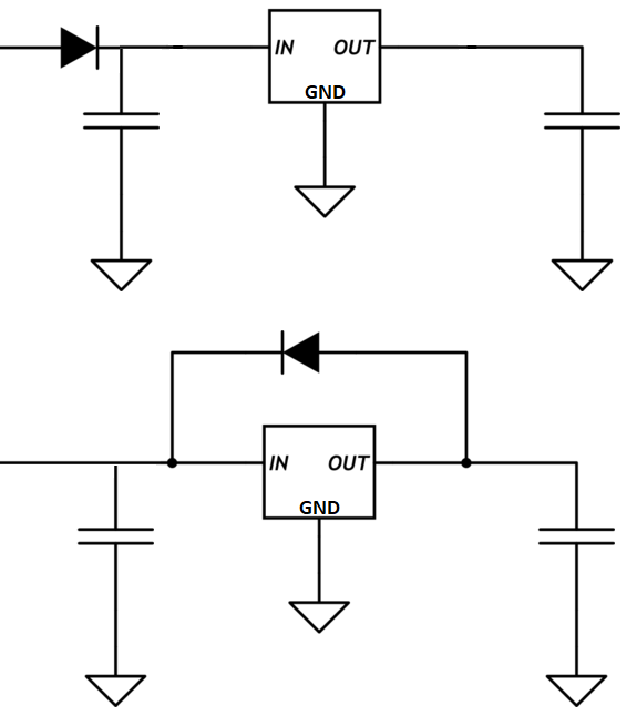
2.  We get a bit worried reading 'This reverse current flow can cause damage to the device. Limit reverse current to no more than 5% of the device rated current for a short period of time.' 
a) What is the suggested way to achieve this current limiting? We are limited in board space and would gain from the small package of TPS7A03, but would like to avoid having to add supporting components for current limiting.
b) It is stated that 'reverse current can possibly flow'. How should one estimate the actual reverse current (to then judge if it is >10mA or not)? Simulation?
c) What would be an example of 'a short period of time'?

Thanks!

  • Hello,

    1. There is only the P-version at this time.

    2. The statement regarding reverse current provides customer recommendations on what values can be provided without damaging the internal CMOS pass element body diode.  When Vout is larger than Vin, current can flow from the output to the input through the body diode. In typical CMOS linear regulators the body diode is not sized to withstand significant amounts of current.  This is the origin of the statement "limit reverse current to no more than 5% of the device rated current for a short period of time". 

    With a sufficient ramp down rate on Vin, and a sufficient output capacitance on Cout, the active pulldown will not be able to sink enough charge from Cout to GND before the input voltage drops to zero volts.  In such a scenario (Vin = 0V, Vout > 0), the body diode will still be forward biased and current will flow from Vout to Vin.  Exact values of time are highly dependent on customer applications, and depend on the effective output capacitance, ramp rate of Vin down to zero volts, value of Vout, and active pulldown value (which itself has some small variation).  A simulation can be helpful to measure the reverse current, or possibly a worst case analysis if enough information on the variables listed above is understood.

    "A short period of time" is also dependent on the customer application.
    The body diode is parasitic and not by design; as such it is lossy and can rapidly heat up with enough reverse current.
    If the power loss across the pass element is too large it will overheat, without any method to stop it (the thermal protection does not prevent reverse current flow).  Higher thermal resistance will cause a failure more rapidly than lower thermal resistance.  As such, a high quality heat sink using plenty of thermal vias attached to surface and internal GND copper, will help protect the device under reverse current flow.

    If your application may encounter the situation where Vout>Vin we recommend placing a reverse current blocking diode in series with the LDO to protect it from being damaged. Below are the two most common ways of protecting a device from reverse current.

    Thanks,

    - Stephen

  • Thank you for that thorough answer.

    3. Parts with active discharge have this warning about possible reverse current damage in the datasheet, commenting that this risk of damage exists despite the active discharge feature. However, is it still correct to understand that the risk of reverse current damage is not larger with those devices than other LDOs?

    4. A key example for us is to compare TPS7A03 with TPS797. Reverse current conduction is mentioned in the TPS797 datasheet as well, but it is not clear to me whether it is talking about the same level of risk or if it is saying that it is further handled in TPS797. It does not mention for insance 'damage' or 'limit to less than 5% of rated current', but is it really saying the same thing as the TPSA703 datasheet? In short: would we need to care about reverse current handling just as much (or more) with TPS797 as with TPS7A03?

    Thanks!

  • Hello,

    3. Yes, you are correct. 
    Keep in mind that some devices have inherent reverse current protection due to the topology of the LDO.
    If the internal pass element is a PNP transistor, for example, it has inherent reverse current protection and no external diode is necessary.
    Please see the following article for reverse current protection in CMOS based LDO's.
    https://e2e.ti.com/blogs_/b/powerhouse/archive/2018/07/25/ldo-basics-preventing-reverse-current-in-ldos

    4. Treat both devices the same with regards to reverse current.  The differences in the datasheet are with regards to when they were updated.  The language you see in the TPS7A03 is the language we have adopted more recently for our newer datasheets, and is similar to the guidance we are providing on this E2E forum.  The risk assessment of reverse current for both devices is the same.

    Thanks,

    - Stephen