This thread has been locked.

If you have a related question, please click the "Ask a related question" button in the top right corner. The newly created question will be automatically linked to this question.

UCC27211: Driver failure

Part Number: UCC27211

Hi All,

I have recurrent failure problems with the subject IC. It is implemented in a motor control driver that works mainly in breaking modality transferring power from a three-phases PMA to a 28VDC load and battery.

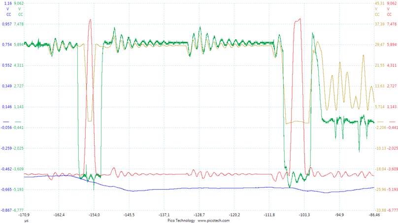
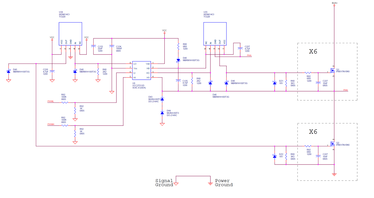
At low load there aren’t problems, but increasing output and/or phase current sometimes a UCC27211D breaks off. Herein after some screen shots (red trace: low side gate signal shifted down of 4V, green trace: high side gate signal shifted down of 4V, ocher trace: PHA to Power Ground voltage (please refer to the enclosed schematic), blue trace: current outgoing PHA terminal and base schematic.


It is observed, at a certain point, that the high gate signal (detected directly on the pins of a mosfet), immediately after switching on the high side switch, drops sharply and reaches a value such as to bring the operation of the switch itself – one would say – in linear operation, but this is not explained since the current flowing in the PHA node (about 700A) flows in the switch towards the BUS+ terminal (from the Source towards the drain) and therefore you should still see the Vds of the high side switch rise to the voltage of BUS+ (battery voltage) minus the Vf of the body diode (give a look to situation of the previous PWM cycle).

In subsequent switching the driver behavior seems compromised and after about 1.5ms the final break of the bridge leg occurs.

As you can see in the schematic, the feeding of the upper sections is obtained by boostrap. The maximum modulation in the screens shown does not exceed 95% (the correct charging of the bootstrap capacitor is however guaranteed). The dead time is 2µs. The switching frequency is 20kHz. From the point of view of the PWM modulation pattern there are no errors.

Waiting for your opinion I thank you in advance.

Best Regards

Flavio 

  • Hello Flavio,

    Thank you for the interest in the UCC27211. I see that the UCC27211 is driving the input of the IXDN614 which is driving the MOSFET Vgs. The waveforms are showing the high side MOSFET Vgs which is driven by the IXDN614 where you indicate the concern of the high side drive failure.

    Have you confirmed that it is the UCC27211 that is the concern, and not the IXDN614? Have you confirmed replacing the UCC27211 only resolves the issue?

    The UCC27211 driver output is the input to the IXDN614, can you confirm if this signal is as expected during this behavior?

    The schematics show Schottky diodes on the UCC27211 HO to HS and the IXDN output to ground. Can you confirm these diodes are located close to the driver IC pins? These diodes can help limit voltage transients on the ICs if they are placed close to the IC pins.

    Can you provide scope plots of the UCC27211 HO output in the behavior condition you provided, as well as IXDN output,  and UCC27211 LO output? Try to get a differential measurement of HO to HS close to the driver pins.

    Regards, 

  • Hello Richard,

    Yes, I confirm that the problem seems to stay on the UCC27211. When I replace the UCC27211 the board starts to work again (until next failure of the UCC...).

    Signal at the input of IXDN614 is correct.

    I also confirm that protection diodes are close to UCC27211 (less than 10-15 millimeters far from the IC).

    At the moment I haven't the scope plots that you requested. I'll try to get them on next days.

    Regards

    Flavio Pozzobon

  • Hello Richard,

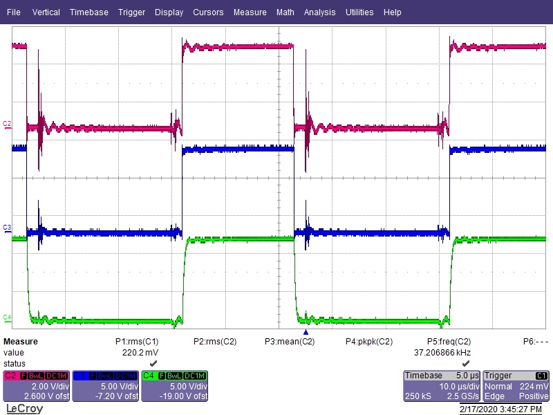
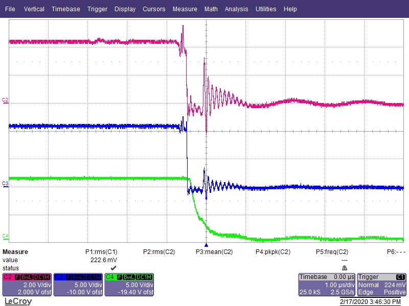
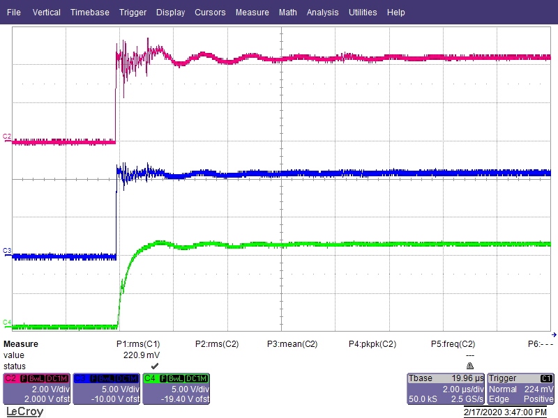
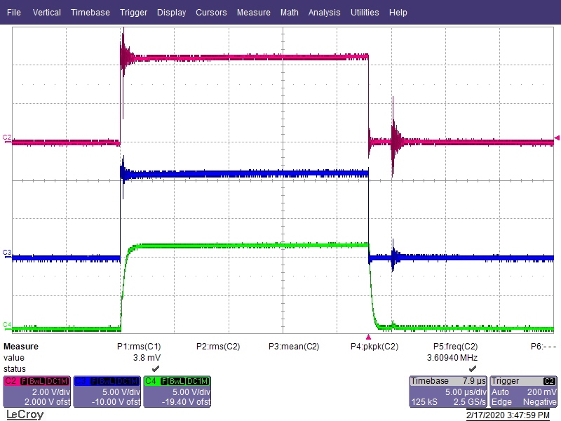
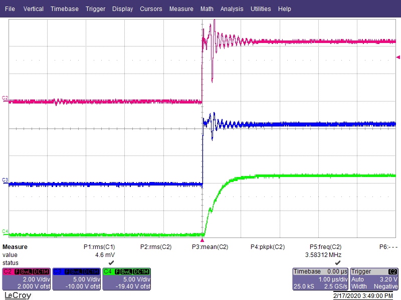
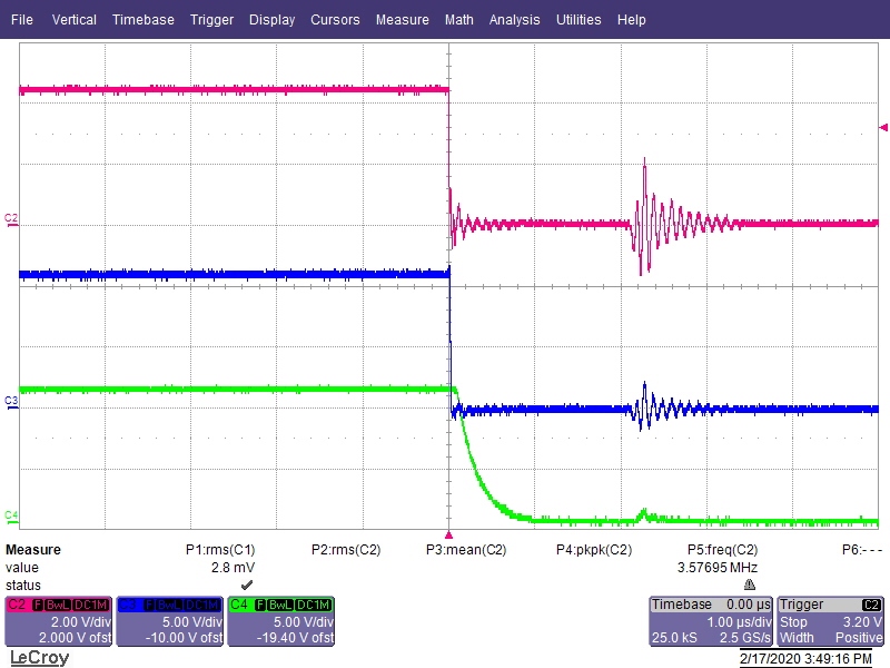
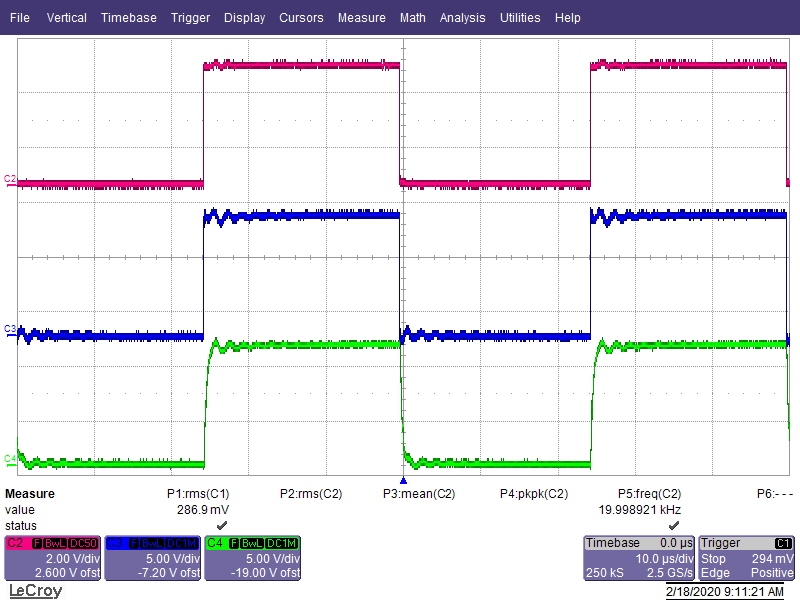
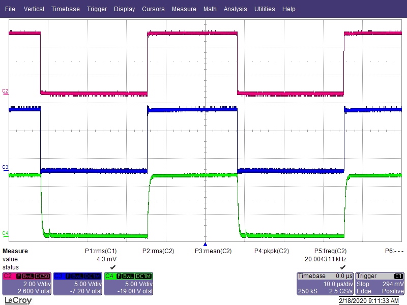
    Here below you can find some scope plots. The channels legenda is:

    CH2: UCC27211 input signal

    CH3: UCC27211 output signal

    CH4: Mosfet gate signal

    First three plots refer to a 290A drain current, last three are at no load condition.

    Best Regards

    Flavio Pozzobon

  • Hello Flavio,

    Thank you for the additional scope plots. These are much more clear regarding the driver waveforms.

    Although it is possible there is high frequency noise spikes form the scope test setup, it looks like there can be noise spikes on the driver input that can result in false triggering. Driver output response and resulting power train response to false triggering on noise can result in conditions that can stress the IC.

    Can you add a small RC filter to the driver inputs to see if the operation improves? I see you show 100 Ohms in series and 1K Ohm to ground. Can you place 33pF and try up to 100pF on the LI and HI input pins to VSS, place the capacitors as close to the IC pins as possible. This will reduce the high frequency voltage spikes and not affect the delays significantly.

    Regards,

  • Hello Richard,

    I have changed the passive probe on CH2 with a differential active probe.

    As you can see, now signal (CH3 and CH4 too) is cleaner and the high frequency noise is strongly reduced.

    With load (300A):

    Without load:

    At this point I suspect a problem on the ground path. To be precise, there could be a voltage gradient between pwm controller ground, UCC27211 ground and source of low side mosfets that hurts the driver IC.

    Regards

    Flavio Pozzobon

  • Hello Flavio,

    The waveforms seem much cleaner with the revised scope setup. Regarding the ground path, there is likely ground bounce occurring from the MOSFET source to the controller ground. I confirmed the UCC27211 has a negative voltage rating on the LI and HI pins, in case there is any negative voltage undershoot, the pins are rated for -10V abs max. Another possible point of stress to the IC is if there is driver output negative undershoot, which the diodes from the driver outputs to ground will help limit. I think you confirmed they are close to the driver IC pins. Also confirm the diode from the INx driver output to ground, is close to that IC pins.

    When the UCC27211 driver is damaged, does it seem it is the low side driver, or high side driver?. Confirm that the HB-HS bias voltage is within the IC ratings of <17V. Are the scope plots the low side driver, or high side driver with HO-HS differential?

    Regards,

  • Hello Richard,

    Damaged driver seems to be the high side one (during failure low side signals look correct) and I confirm the HB-HS voltage within IC ratings.

    Last scope plots refer to low side driver.

    Could be a internal shift level problem? I watched to the following video https://training.ti.com/gate-driver-training-series-gate-driver-operation-high-dvdt-and-didt and, if I'm not wrong, something is mentioned regarding shift level troubles.

    Regards

    Flavio

  • Hello Flavio,

    Thank you for the clarification on the scope plots. Regarding the recent comments, and reference to the training which I am familiar with and have contributed, there are a number of operation concerns relating to high dV/dt in the power train.

    High dV/dt on the power train switch node can lead to driver and gate drive  issues including Vgs negative voltage from MOSFET miller charge, and exceeding the HS pin dV/dt specification.

    Confirm the slew rate of the switch node, or driver HS pin is within the 50V/ns rating in the datasheet. The dV/dt is most commonly reduced by increasing the gate resistance, in the case 6.8 Ohms, to reduce the Vgs slew rate.

    Too see if there is a dV/dt related issue, try as an experiment increasing the gate resistance of 6.8 Ohms to 2x the value as a starting point. Since you have capacitance on the gate to source, this capacitance could be increased to have the same effect of reducing the Vgs rise and fall times.

    Regards,

  • Hello Flavio,

    It has been a while since the last post. We will assume you have resolve the issue, if there are any more questions you can post them on this thread.

    Regards,

  • Hello Richard,

    Due to the short time available I have changed the subject drivers with galvanically isolated ones and put them on flying PCB. Now the board is working correctly and pointed me to analyze deeply the ground paths layout.

    Thank you very much for the effort on trying to solve the problem.

    Best Regards

    Flavio Pozzobon

  • Hello Flavio,

    Thank you for the update. Isolated drivers can help in two main ways, ground bounce which may lead to noise on the driver inputs, and negative voltage tolerance that is improved over monolithic drivers, especially the negative switch node voltage spikes.

    If you get some insight into the potential ground routing issues, and want help again to use the more cost effective half bridge drivers, you can post your questions on a new thread or to this one again.

    Regards,