This thread has been locked.

If you have a related question, please click the "Ask a related question" button in the top right corner. The newly created question will be automatically linked to this question.

TPS61176: Output current stability of TOS61176

Part Number: TPS61176

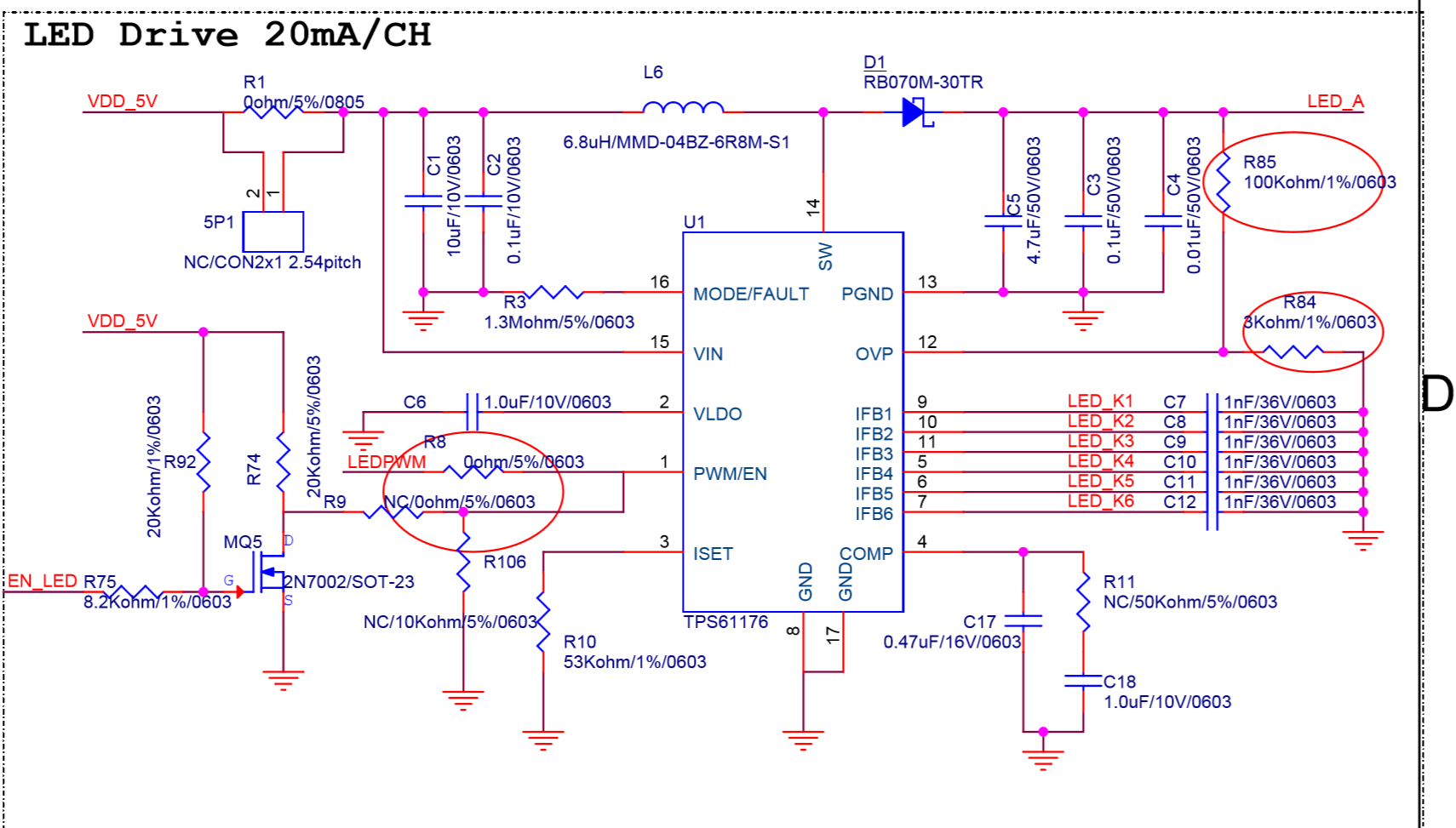
For TPS61176 chip, the current EN pin voltage we use is about 1.7V (as shown in the red box below). Under this condition, when the output channel is > = 3 (the total output current is about 60mA), the problem of backlight flash caused by unstable output current is likely to occur (there is no flash problem for 40mA output).          

When the EN pin voltage is increased to 1.8 ~ 3.3, the flicker will disappear. In the specification, the EN pin voltage is more than 1.2V. Please help to see if there are restrictions in other parts of the chip.Output current stability of TPS61176.pptx

  • Hi Sir,

        Thanks for the detail description of the question, I guess it may have triggered the current limit or the inductor may get saturation, Could you provide the waveform of "Vin", "Inductor current" and "Vout" of the abnormal phenomenon? You need to make sure the "EN" pin voltage is larger than 1.2V, you'd better add some margin for the mass production.

    Regards

    Sean

  • Hi Sean,
    Can i email you directly?

  • Hi Sean,

    How do I test the waveforms of Vin and Vout to ground?

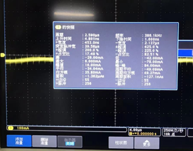
    The L6 current test is as follows.

  • Hi Sir,

        Put the "Vin", "Vout" and "inductor current" in same page, Please zoom out the inductor current waveforms, it seems the inductor current is not stable.

    BR

    Sean

  • Hi Sean,

    I want to know how is the Vin and Vout waveform tests grounded?

  • Hi Sir,

        If you worry about the Grond is not clean, you can try with a Differential probe or use two probes to minus to get the differential value.

    BR

    Sean

  • Hi Sean,

    We use TPS61176 to drive the backlight, the load is If = 60mA, Vf = 20V, and half of the screens are found. Help to confirm what may be the reason?

  • Hi Sean,

    After the abnormal PCBA is powered on, the LEAD current value fluctuates back and forth between 56 ~ 60.5mA, and the screen shakes; after about 7 seconds, the LEDA current value will stabilize at 60 (the fluctuation range is within 0.03). The jitter returned to normal.However, it is unstable, and the picture may be shaken after testing for a period of time.

    After the abnormal PCBA is powered on, the LEAD current value fluctuates continuously between 56 ~ 60.5mA, the screen shakes, and the scene is continuous.

    L6 material test data is as follows:

    Category Sample description Quantity L   (μH) L   IDC (μH) Isat(%) DCR (mΩ) RS     (Ω) judgement
    6.8±20% ﹢0A ﹢2.1A ≦20% 162TYP 178Max 1.5Max
    1# L6 material disassembled from the splash screen 10 7.23 7.22 6.13 15.12% 158.8 1.15 OK
    2# L6 new material 10 7.38 7.36 6.13 16.71% 158.06 1.11 OK

    We want to know what affects PCBA so unstable?

  • Hi Sir,

         Please remove C7-C12 and test again. Or change with 33pF.

    BR

    Sean

  • Hi Sean,

    After removing C7 ~ C12, the LEDA value fluctuates and the test will still flash.

    Test after changing C17 to 1uF, LEDA current value fluctuates, splash screen

    Do you mean to change C7-C12 from 1nF to 33pF?

    We found that this board is normal for testing the backlight of 2 strings of lights, but the backlight of testing 3 strings of lights will show about 50% flicker (LEDA fluctuation)

    Because the 3-string lamp project requires the LEDA current to be 60mA, can the current of the LEDA be stabilized by changing the specifications of the Chip component and is the LEDA current approximately equal to 60mA?

  • Hi Sir,

        So the only method you have found is increasing the voltage on “EN” pin, does this really solve all the problem?

        How about  increase the C17 value to 1uF to narrow the bandwidth or short R11 and connect C18?

    Regards

    Sean

  • Hi Sean,

    After C7 ~ C12 is removed, the screen still flashes.

    Is it necessary to verify the experiment of C7 ~ C12 changing from 1NF to 33pf?

    Short R11 and connect C18, which means that both R11 and C18 need to be short circuited?

  • Hi Sir,

        It is really strange, so if you increase the voltage of "PWM/EN" pin, it will solve all the problems? Can you make sure that? If you can make sure that I will inform this to our engineers. And if this is really helpful, so please increase the voltage of this pin.

    Regards

    Sean

  • Sean,

    After replacing C17 with 1uF, the product has not been improved; 

    The shorting of R11 and C8 is also the same without improvement.

    Increasing the voltage of "en" pin can really solve the problem, which my colleague has verified.

    At present, there are many 2016-2018 products in this situation.I don't know whether it was caused by product aging and function degradation or whether it was also caused by this problem before

    The backlight of 2 series lights is normal, and the backlight of 3 Series lights is faulty.

    Is there any way to stabilize Leda current at 60mA?

    Can you help to see if the layout of PCB is defective?

  • Hi Sir,

        Could you please send us the PDF format of the layout since it is not convenient to check the format that you have sent. Thanks.

        I think for this situation, it better to have a call to talk about the problem, please contact TI sales or FAE. Let's work out this together

    Regards

    Sean

  • Hi 

        When you do the test with two channels or three channels, how do you deal with other channels? have you connected them to ground? 

    Regards

    Sean

  • Sean,

    Yes, the other unused channels are grounded.

  • Hi Sir,

        As we have discussed in the meeting, you can try to add the cap value to the "VLDO" pin and check if there any improvement.

    BR

    Sean

  • Hi Sir,

         1. From the test results, it seems the problem is that the output voltage is really big, could you split the front power stage and use the external power supply instead of onboard "VDD_5V" and test again? thanks.

        2. What's the dimming frequency you have used and under which PWM duty cycle you have observed the flick issue?

    BR

    Sean

  • Sean,

    Where can I see that the output voltage is very large? I hope my test results don't mislead you.

    Change point                                 Flicker voltage Other contents
    Original board <0.88V 1.52~1.64V Flash screen
    LEDA current value fluctuation
    C6 changed from 1uF to 4.7uf <0.88V 1.46~1.65V Flash screen
    LEDA current value fluctuation
    Restore C6,
    C5 parallel 2 10uF
    <0.9V 1.51~1.68V Normal screen display
    LEDA current about 87 ~ 89mA
    remark Measurement method: R8 disconnected, R8 close to U1 1pin and J31 pin12 charged  

    Dimming frequency is 22K ~ 30K, PWM duty cycle is 100%

    Remove R1, connect 5V voltage to pad near U1 and 12pin of J31, abnormal board (flicker screen, LEDA current fluctuating in 58-59) returns to normal (normal screen display, LEDA current 60.42-60.43mA)

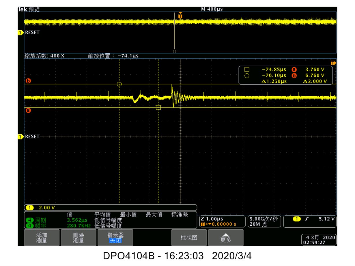
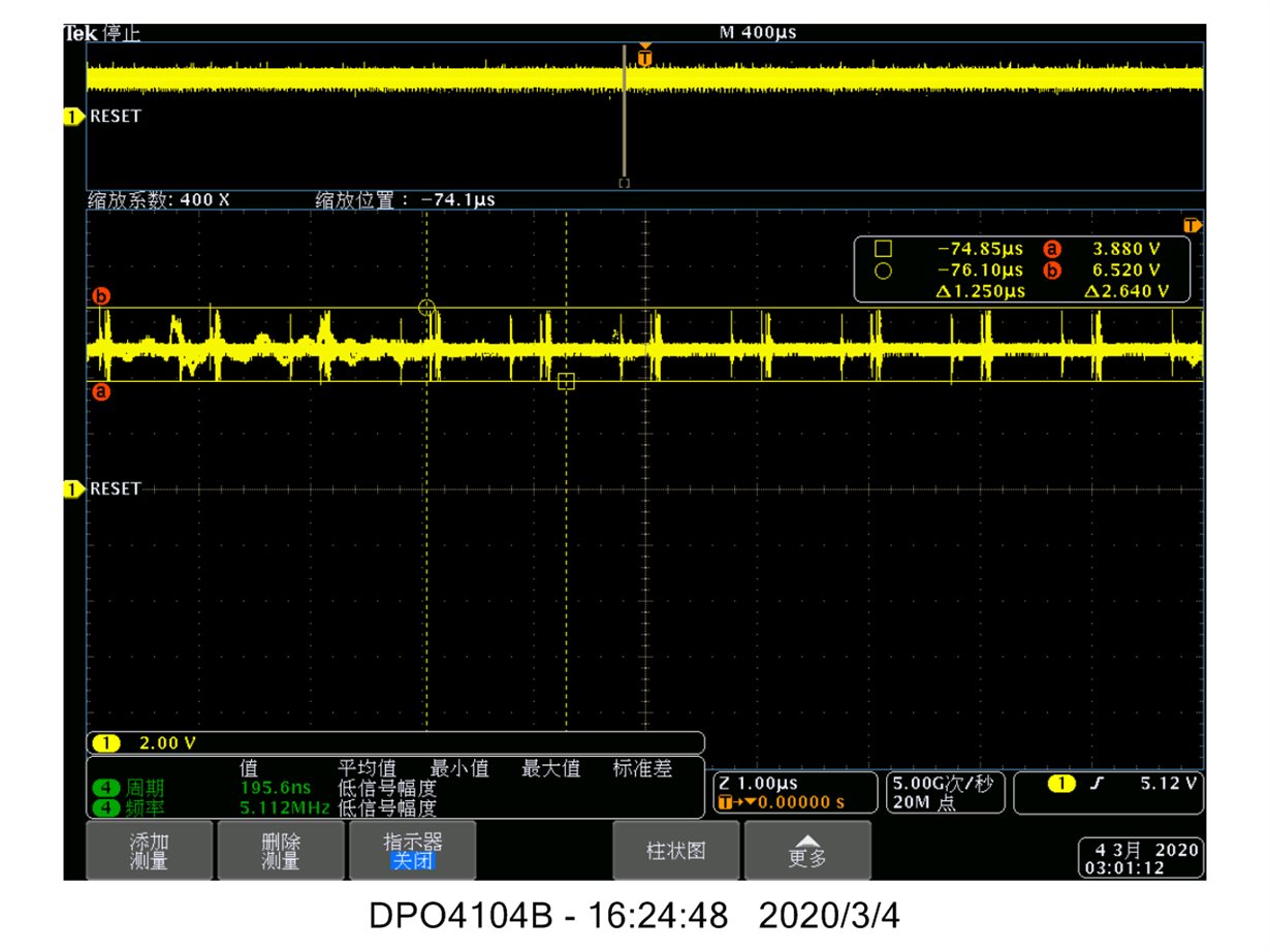
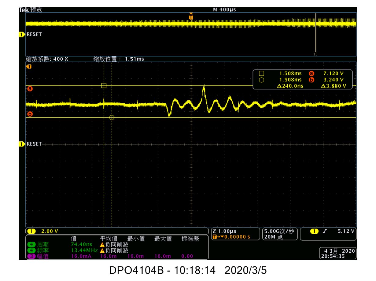
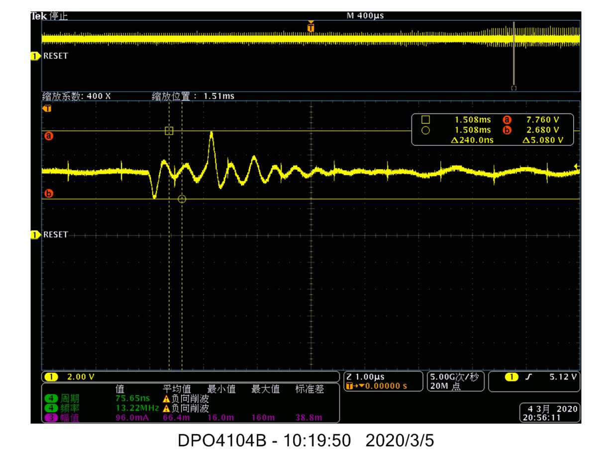
    Figure 1: VDD waveform of normal products


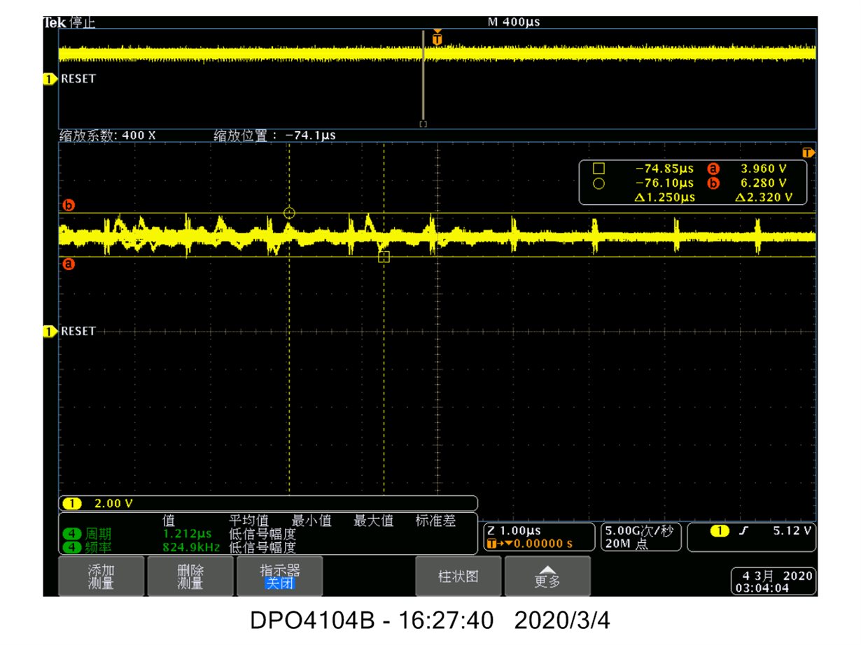
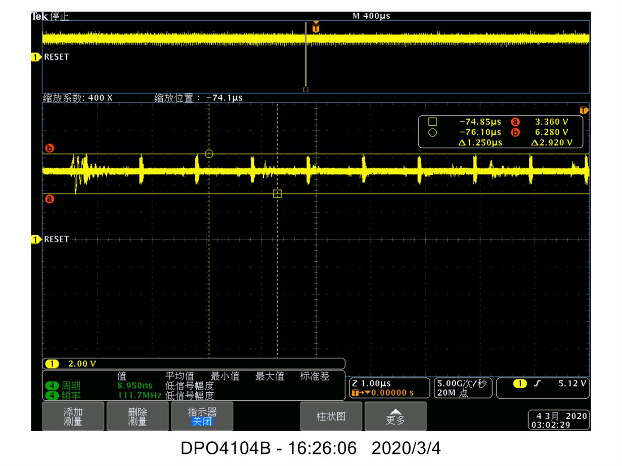
    Figure 2: VDD waveform of abnormal products

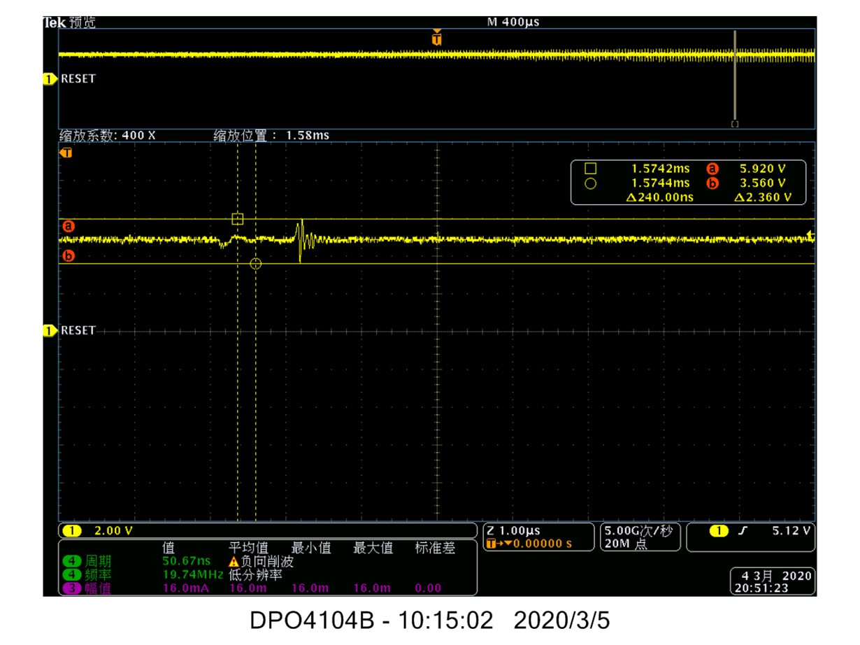
    Figure 3: VDD waveform of abnormal products


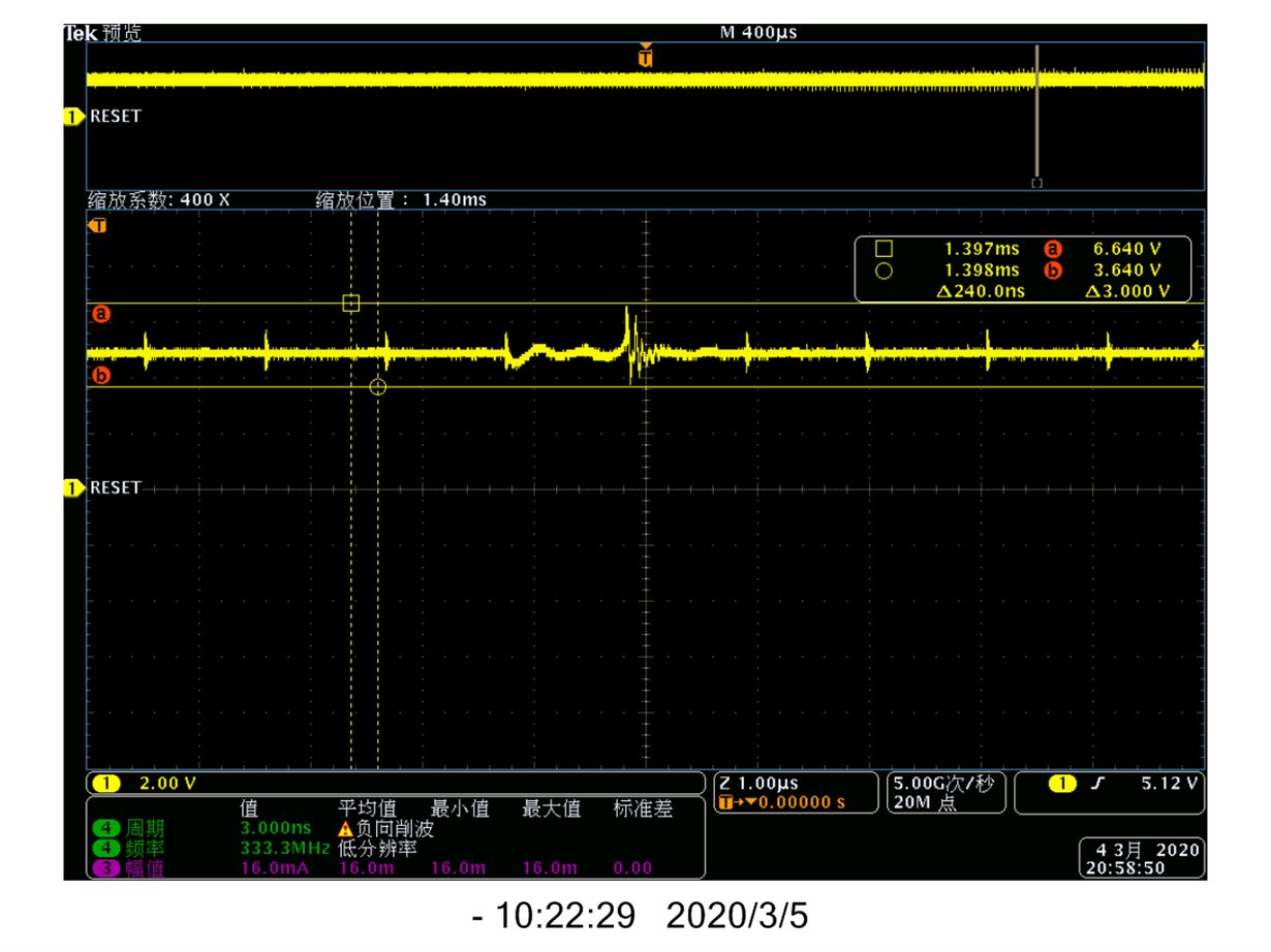
    Figure 4: VDD waveform of abnormal products

  • Hi Qing

    As we discussed with E-main, It seems that the original “VDD_5V” form the board is not very stable and it leads to the flick issue of the LCD panel. 

    BR

    Sean

  •  Sean,

    I measured the VDD voltage of normal board and abnormal board, and found no obvious difference.

    For details, please refer to the four wave charts added in the previous reply.

  • Hi Qing,

        How to explain why you have used the external power supply , all flick issue has gone? I think that's the problem.

    BR

    Sean

  • Sean,

    I tested the waveform of 5V external connection between good products and abnormal products.

    The input waveform of power box also fluctuates greatly

     Figure 1: wave form of 5V external connection of normal products


    Figure 2: waveform of 5V external power supply for abnormal products


    Figure 3: waveform of 5V external power supply for abnormal products


    Figure 4: waveform of 5V external power supply for abnormal products

  • Hi Qing,

        For the abnormal product, it seems the fluctuates greatly than the normal board, but you need to check the difference between the external power rail and on-board power rail with the abnormal products. 

       From the above phenomenon, I think the problem is that your on-board power rail is not very stable and it will lead to the unstable voltage on the "EN" pin, so it may lead to the device flick.

    BR

    Sean