This thread has been locked.

If you have a related question, please click the "Ask a related question" button in the top right corner. The newly created question will be automatically linked to this question.

UCC27714: Ringing at HO Pin

Part Number: UCC27714

Hi, 

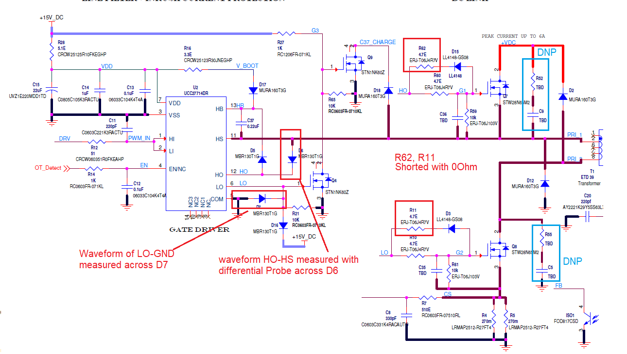
I have a power supply with 2 S/W Forward Converter Topology and i am using UCC27714 as Gate Driver. 

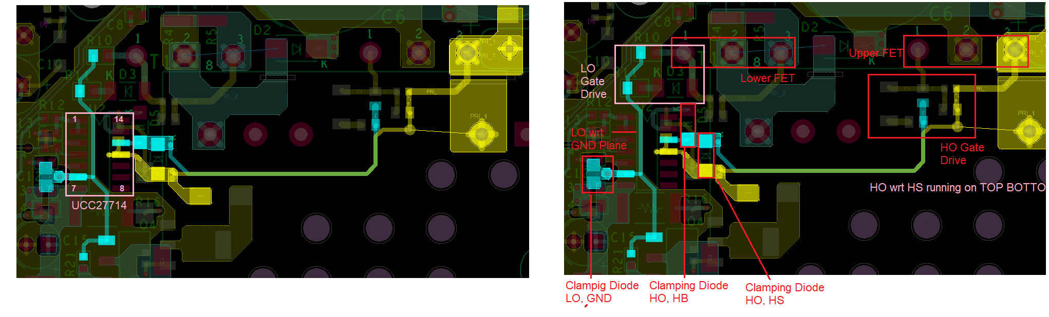
Attached is schematic and Layout of UCC27714. 

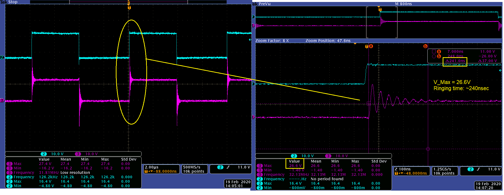
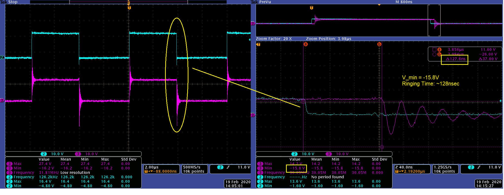
I am observing too much ringing at HO-HS Pin. 

 have measured it with differential Probe and attached is the waveform of the same. ii observed catastrophic failure of both Upper and Lower MOSFET, Most probably due to ringing at Gate Terminal. 

wave forms i have captured are taken when MOSFET switching is disabled. 

What would be the possible cause of such ringing at HO-HS pin. 

Waveform at LO_GND looks much better as compared to upper. i captured wave forms  on multiple boards (3 nos) the result is consistent. 

Thanks for help.       

  • Hello Abhishek,

    Thank you for the interest in the UCC27714. The ringing that you can see on the gate drive waveforms is a result of the gate drive loop parasitic trace inductance and parasitic capacitance in the circuit. The parasitic inductance of the trace from the driver to the MOSFET gate, and MOSFET source back to the driver ground reference, in this case HS is in the gate drive current loop. I am surprised you are seeing the same high ringing on the turn on edge and turn off edge, since there is a 47 Ohm turn on gate resistance, and 0 Ohm gate resistance. Keeping the gate drive trace lengths as short as possible reduces this inductance. Also, increasing the trace width will reduce the parasitic inductance.

    Can you confirm there is not a probe connection issue, which is resulting in excess ringing measurement?

    Since you are using a two transistor forward, can you confirm the HB-HS bias is as expected to ensure the correct HO operation. There is a potential concern in charging the boostrap bias with a 2 switch forward. Refer to the UCC27714 datasheet, Figure 49 for the 2 switch forward example.

    Regards,

  • Hi Richard, 

    As you can see in my post, i am capturing waveform across Clamp diode of HO not at G-S of MOSFET, so gate resister is not coming in picture and hence it will not damp out any oscillations.

    Also i checked it on multiple boards (3 nos) observed same ringing with same frequency ~30MHz.  

    For the Trace length you can see that, length of HO-HS trace is more as compared to LO-GND, but these 2 traces are taken from Top, Bottom  exactly superimposing on each other. i can not reduce trace length as of now so have to deal with this issue. 

    i had connected MOSFET but we had failure of MOSFET at very low load (During Burst Mode operation). Ringing is of ~30MHz, so adding small ferrite bead (0603) in gate path can it be a option? 

    I will check the MOSFET Switching at low DC Voltage to avoid catastrophic failure. will update you with observations. 

    Regards

    Abhishek 

  • Hello Abhishek,

    Ferrite beads can be very effective a reducing high frequency ringing on the gate drive signals. Look for a bead that has high impedance at high frequency, ex 10MHz.

    Regards,

  • Hi Richard,

     It looks like that the ringing we observed on HO-HS was indeed a probe measurement issue. 

    i used battery operated Scope with high bandwidth to measure the same waveform and it looks just fine. No need to use Ferrite Beads. 

    We observed propagation delay of  ~90nsec but it is fine and as per the datasheet. 

    we are able to load power supply successfully up to 300W and will continue up to 500W. 

    Will post update or query  on the same thread. 

    Regards

    Abhishek