This thread has been locked.

If you have a related question, please click the "Ask a related question" button in the top right corner. The newly created question will be automatically linked to this question.

LMR33630-Q1: PCB Layout

Part Number: LMR33630-Q1

Hi Team,

My customer now uses our LMR33630-Q1. 

Actually I have helped them to review twice about the LMR33630-Q1...

Based on my advice, they have changed  a lot. You can't image how xx the first version is...

However, because they used the competitor before and now change  this part to TI solution. So the space is very limited.

I will ask them to add the standard 8 Cin+Cout as datasheet suggested.

Any other advice or comment about the layout?

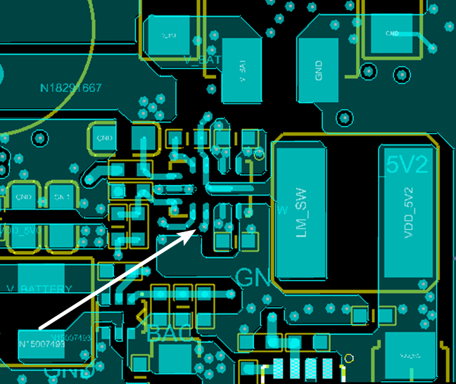
Here are the third version:

  • Hi,

    The small input capacitors, boot capacitor and FB resistors look good if the Vout-FB return path is away from SW node. If they have a very limited space, it's OK to put bulk capacitors a little far away from Vin-GND pin but still needs the path as wide and short as they can. On output, they also need to have enough capacitors for a certain load. Thanks.