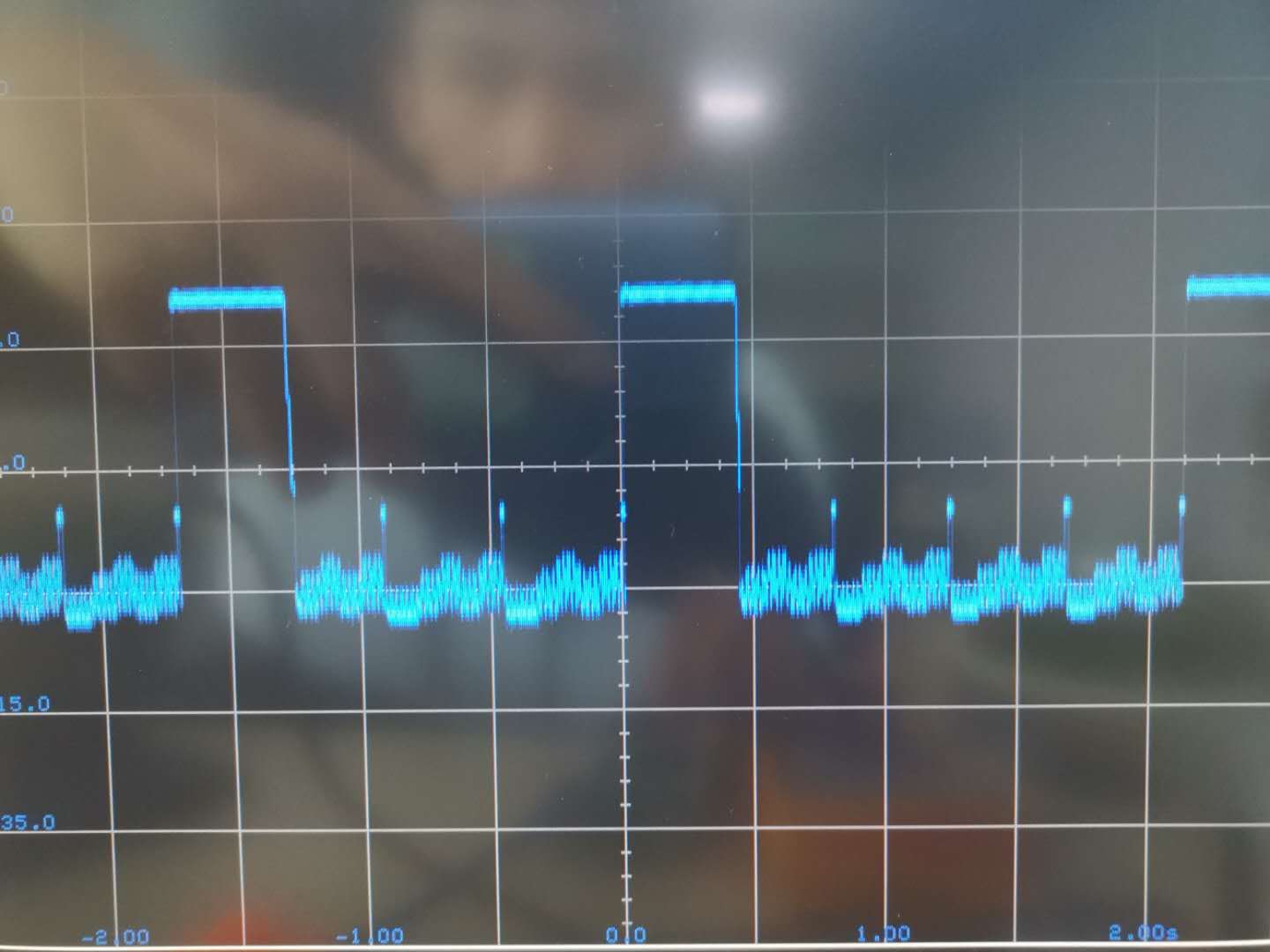
The schematic diagram is designed according to the recommended design. After power on, the board card does not output, and the high and low level of the test den pin is repeatedly switched. The same is true for the primary waveform diagram of the test transformer

-
Ask a related question
What is a related question?A related question is a question created from another question. When the related question is created, it will be automatically linked to the original question.