This thread has been locked.

If you have a related question, please click the "Ask a related question" button in the top right corner. The newly created question will be automatically linked to this question.

UCC28600: TINA example model setup, changing the transformer to a coupled inductor

Part Number: UCC28600
Other Parts Discussed in Thread: TL431

Hi,

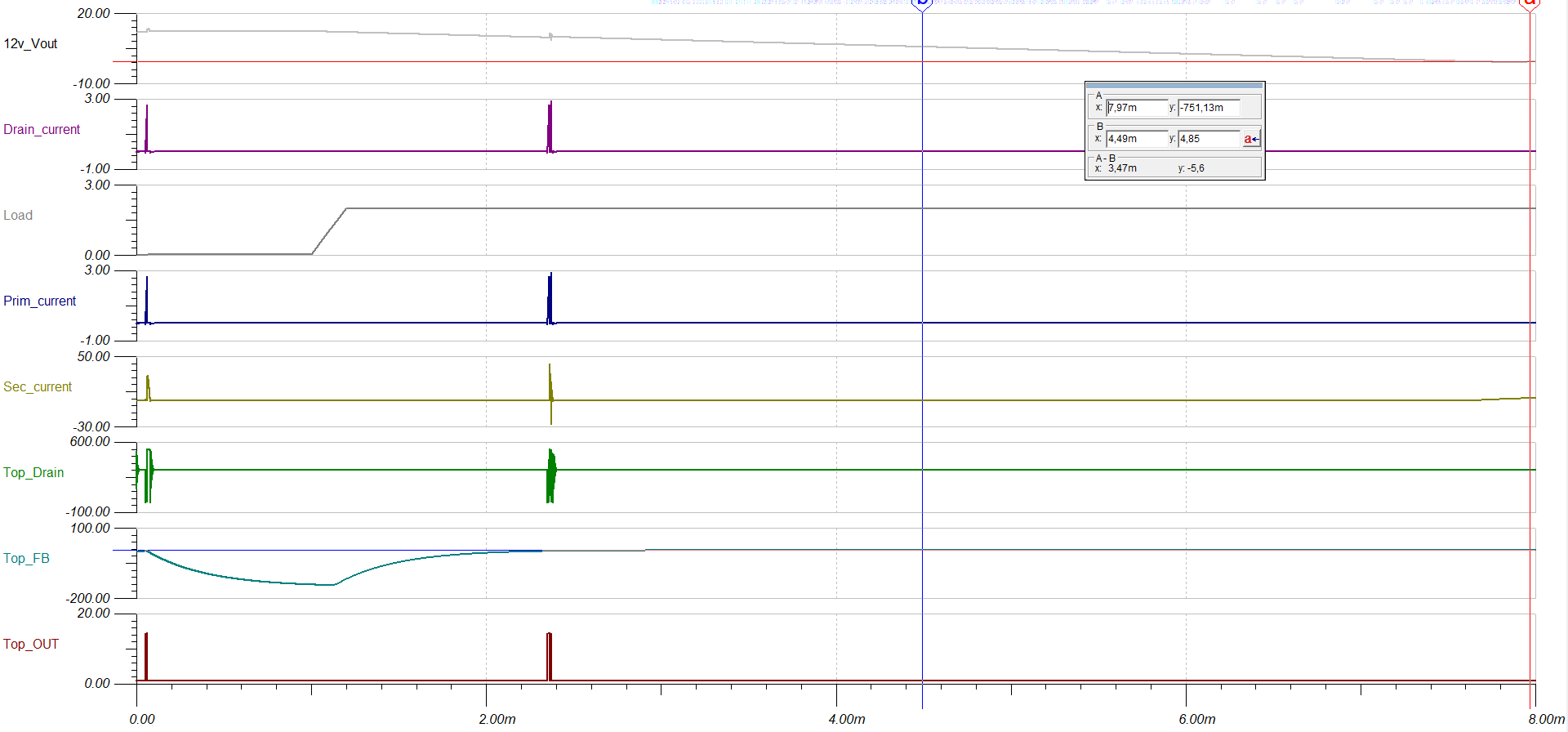
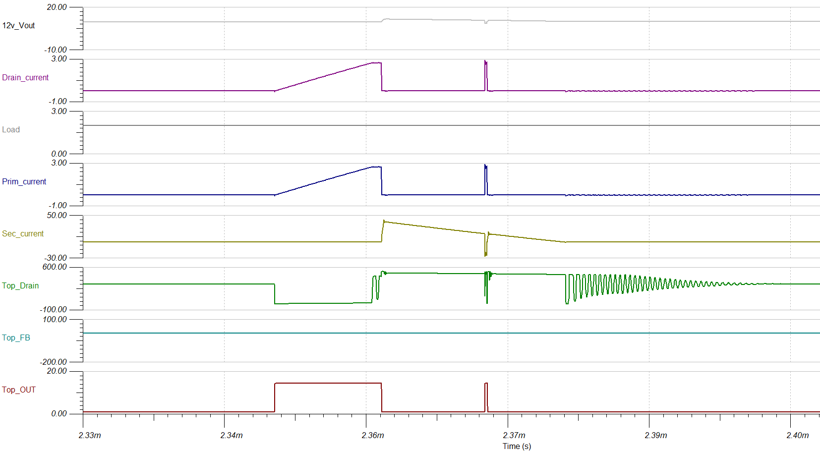
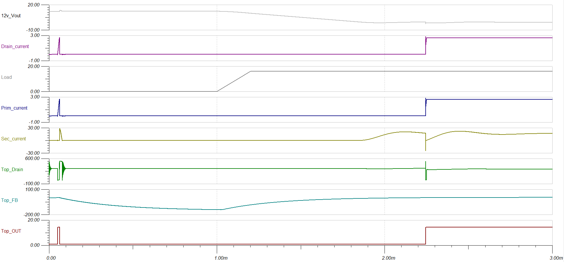
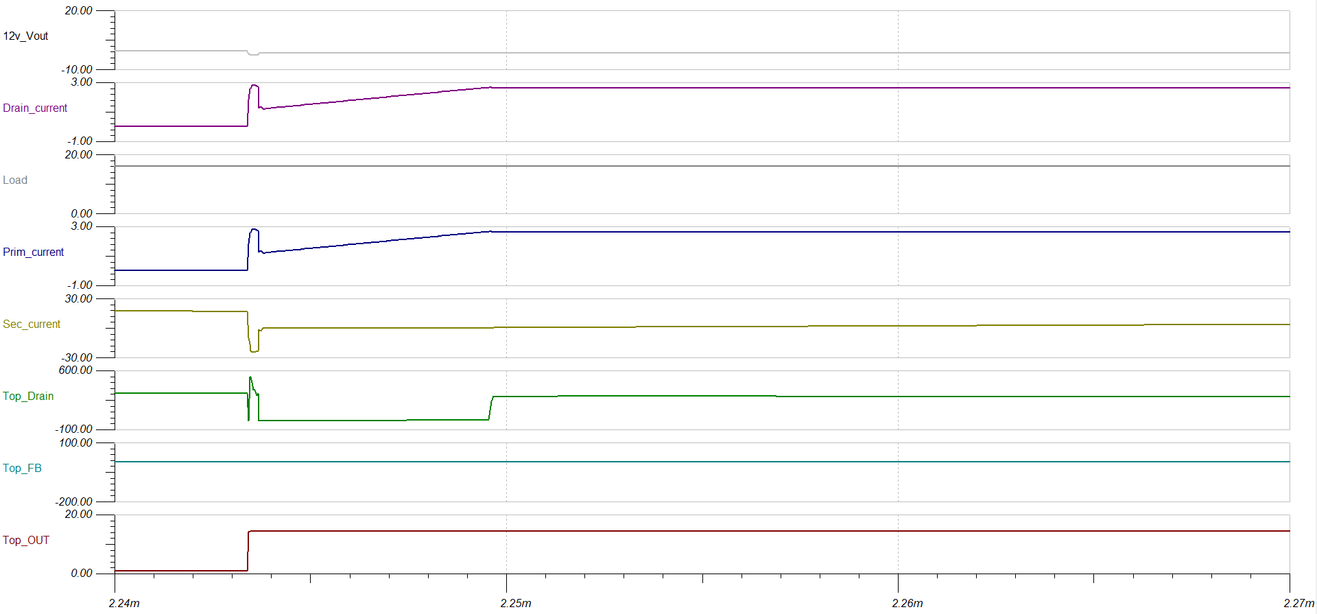
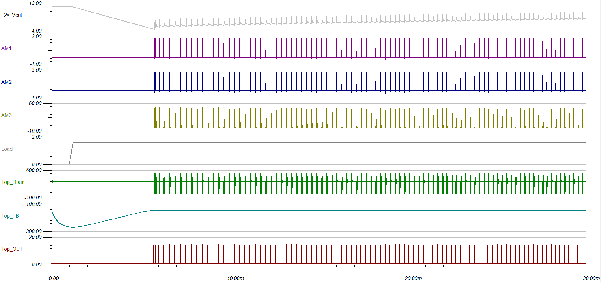
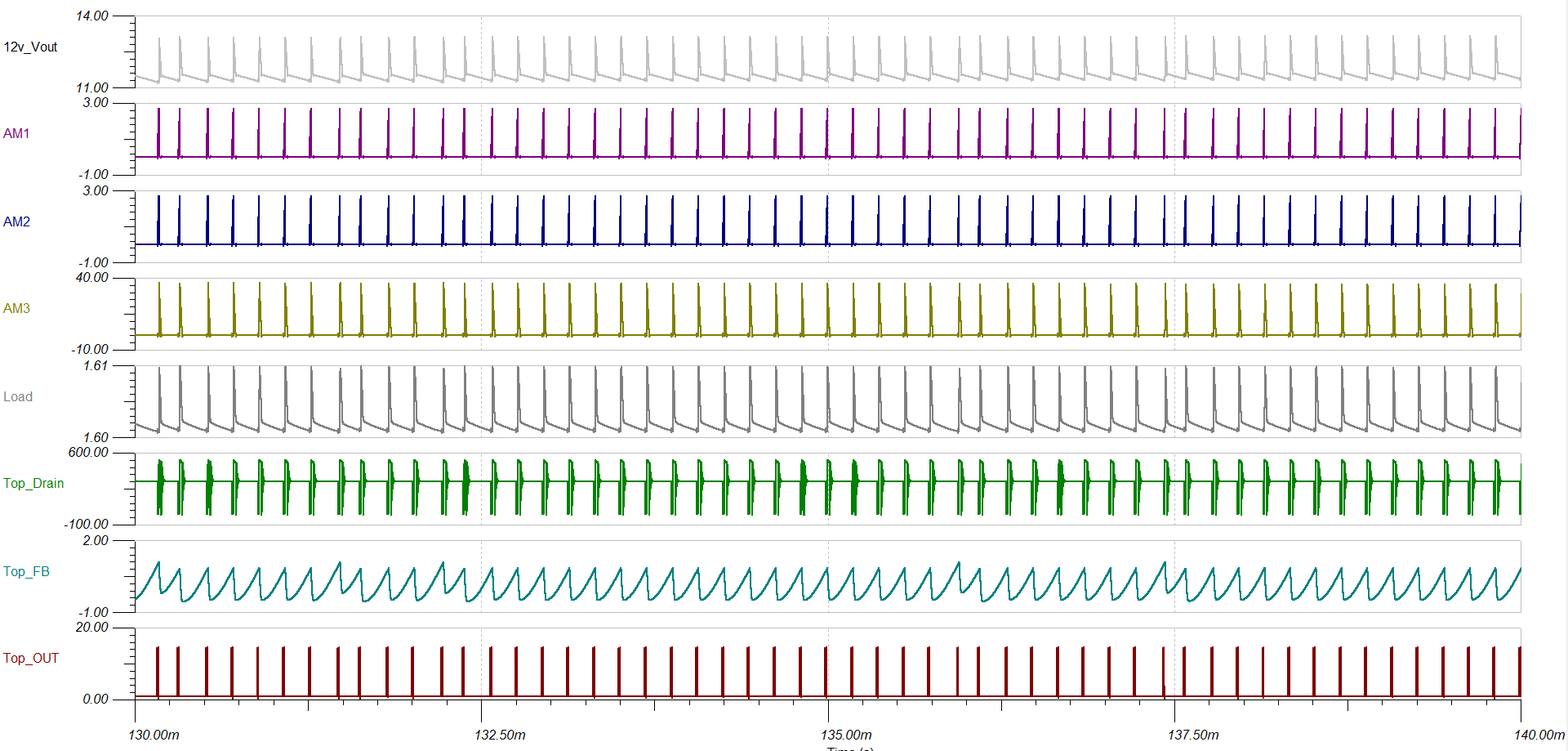
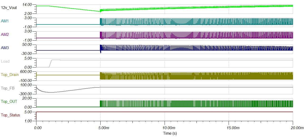
I would like to design a multi-ouput flyback converter based on UCC28600 controller IC. I would also like to simulate the circuit, therefore I was trying to change the transformer to a coupled inductor (because later I will need more than one output) in the given TINA example model to see if it is even possible to simulate the same system but with a coupled inductor with the same properties used with the transformer. Unfortunately, if I use a coupled inductor, the simulation result is completely different than before.

Is there any way to change the transformer to component with which I would be able to simulate successfully a multi-output flyback topology?

Thank you in advance!

Bálint

  • I suggest you simulate just with single output. Then you use cross regulation to understand other output. It is mainly a transformer simulation which you need to build your own model. Basically just to find out the leakages and coupling factors

  • Hey,

    First, I really appreciate your answer, thank you very much! I took your advice and I was trying to simulate the circuit only with one output. Right now, all of the component values have been calculated but the circuit either works in a really weird way, or I get the infamous convergence problem. For example, the weird thing is that voltage top of the current sense resistor has a waveform which is far from ideal, it doesn't have the ramp increase, instead the voltage changes instantly. If the current source is around 4 A, than the duty cycle of the OUT pin looks strange as well. It has a kind of a normal cycle, after that some really thin pulses and it keeps repeating. I attached the current version. Do you have an idea why is it working like this?

    Edit.: I left the given transformer model in the simulation, I just changed its values based on my calculations.

    mine.TSC

  • It looks some setup not good.

    Can you start with the TINA design (attached here, "slum608.TSC") from TI web and change one thing at a time to see which change causing the convergence problem?

    I just ran "slum608.TSC"  and it worked ok.

    slum608.TSC

  • Hi,

    Since then I did what you suggested, and the main reason why the circuit was not working is the incorrect secondary diode I've chosen.

    My problem now is the following: The attached simulation works as expected until 1.4A of load. The problem is, if I go higher than this value, the controller is unable to hold the output voltage on the desired 12V, even though all the values (OVP, current sense etc) have been calculated for 197W output power with 85% efficiency, therefore if the output current would be around 16A, it still should be able to work. Now I'm a bit stucked. I think the chosen OVP resistor values and current sense protection (Rcs and Rpl) have been calculated correctly, I don't really see why the controller stops the operation. Unfortunately, I don't know TINA that well, but my first thought was maybe the diode on the output causes some problems, as the current one is able to handle 1A maximum forward current, but changing that value doesn't help.

    Maybe somehow the state machine starts to work incorrectly? May I ask your help in this regard?

    Thank you in advance!step_by_step.tsc

  • Can you probe each node to see if any hint? Also, when 12V is not held, does it drop or shutdown? If it drops, which means some setup is likely saturated. If shutdown, it means some fault triggered. You need to check one at time.

  • 12V slowly drops, it is quite clear that the controller doesn't put energy from the primary side, so the capacitor on the secondary side just loses its charges and the voltage drops in the same ratio.

    This is how it looks the drop after the load reaches the problematic level.

    And there are weird spikes in the current signal after the 2ms mark if I zoom in.

    This happens at 2A of load. This thing goes even more weird, if I change the load to 16A. In that case the controller keeps the primary side transistor open, and although the voltage on the output drops, the waveforms look really strange after the load goes on.

  • Can you compare your simulation circuit and the original? My review of your circuit looks you removed the feedback loop compensation components on TL431 so your circuit cannot make correct loop compensation.

  • I added the loop compensation as you suggested by following the steps in the "Compensation Design With TL431 for UCC28600" (SLUA671) document. The circuit unfortunately still doesn't work as expected. I can go a bit higher with the current up to around 4A (you can see a picture about a simulation with 1.6A load below), but it is still far from the final 16A. A was also trying to add the Zener network later before Rled, but it didn't help either. Based on the transfer characteristics, the compensation network should do the work, I changed the crossover frequency to 3kHz of Vo/Vcomp, it also meets with all the stability conditions.

    The other really weird thing for me (although maybe I just misunderstood something) is the switching frequency. Shouldn't it work with at least 40kHz bursts? Right now, depending on the load, the switching frequency varies between ~3kHz - 7kHz.

    And the pictures:

    Unfortunately it is quite hard to figure out if it reaches 12V or not, because the simulation stops with convergence problem a lot of times. Sometimes pressing 'retry' works, but I don't know how accurate the result going to be after this error. Also if I don't change anything in the example simulation, but I change the simulation time to 30ms, it doesn't run. It quits with convergence error.

    So back to my circuit: It reaches the target output voltage @1.6A, but during the simulation I had to press 'retry' on the convergence error once.

    At 3.5A at the start it looks like the system operates in CCM, but the controller is a DCM one, so it shouldn't happen right?

    The Bode of Vo/Vcomp

    I also attached the updated simulation circuit.

    5824.step_by_step.tsc

  • How did you decide the loop compensation?

    How did you design your converter parameter values?

  • For the loop compensation as I said I followed the method presented in SLUA671.

    The following MATLAB code shows my implementation

    s = tf('s');
    Rd = 8;
    ESR = 50e-3;
    Rcs = 151e-3;
    Vtl431min = 2.5;
    Vdd = 5;
    Vcesat = 0.3;
    Vf = 0.7;
    Ibias = 1e-3;
    CTRmin = 0.4;
    Rpullup = 20e3;
    Rledmax = (Vout-Vf-Vtl431min)/(Vdd-Vcesat+Ibias*CTRmin*Rpullup)*CTRmin*Rpullup;
    R1 = 10e3;
    Vsample = 2.5;
    Rlower = R1*Vsample/(Vout-Vsample);
    Vin = 325;
    Voutmax = 13;
    Nps = 15.27;
    D = Nps*Voutmax/(Vin+Nps*Voutmax);
    H = Nps*D/(5*Rcs)*Rd*(ESR+1/(s*Co))/(Rd+ESR+1/(s*Co)); %transfer function of Vo/Vcomp
    bode(H);
    Gmid = 10^(12.65/20); %to have 3kHz as cross-over frequency
    Rled = 499;
    R2 = Gmid*R1*Rled/(Rpullup*CTRmin);
    [z,p,k] = zpkdata(H);
    p = cell2mat(p);
    fz = abs(p(2,1));
    fp1 = 40e3; %suggested pole
    fp2 = fp1;
    C2 = 1/(2*pi*R2*fz);
    C1 = 1/(2*pi*R2*fp1);
    C3 = 1/(2*pi*Rpullup*fp2);
    Copto = 2e-9;
    F = (s*R2*C2+1)/(s*R1*C2*(s*R2*C1+1))*(1/(1+s*Rpullup*(C3*Copto/(C3+Copto))))*Rpullup/Rled*CTRmin; %transfer function of compensation network
    bode(F);
    bode(H*F);
    Are you curious about all the converter parameters (transformer parameters etc), or only the ones which needed for the controller (OVP, current sense, Css etc)?
  • I need your converter parameter design too. Since you mentioned your converter entering CCM, this indicates some parameters may need adjustment. One possibility is your transformer may need to adjust.

  • If you designed your converter using the Excel tool on ti.com, please forward your excel design file to me. If you did not use that tool, please first check your design based on that tool, if you cannot find anything wrong, then please forward your excel design file to me. 

  • After changed a few component values, now the simulation model works ok. The modified model is attached along with the simulation result.

    5824.step_by_step_work.TSC

  • Thank you very much. I don't want to look ungrateful, but if I change the load to 16A, it doesn't work. Unfortunately the goal is to have 200W power output.
    Also, could you please explain why did you change the reference voltage and leave C1 from the compensation network?

    In the meantime, I will compare the excel results to my calculation results (I don't want to use the excel, because I'd like to understand what and how one can calculate the necessary values).

  • Your design is not for 16A - you need to make a new design to operate with 16A. Even your current design is not good for 4A before my adjustment. 

    You can add C1 back then you can tune it up to see if it helps or not needed.

    I have just proved the model can work with parameter adjustment. 

  • Because the simulation clearly doesn't work based on my calculations, I thought I give the excel a try, so I can see how a 200W design should look like. I attached the excel file. I also attached the TINA model which has the components values calculated by the excel given by TI. For the compensation network, I used the following MATLAB code:

    s = tf('s');
    Rd = .72;
    Nps = 9;
    Vtl431min = 2.5;
    Vdd = 5;
    Vcesat = 0.3;
    Ibias = 1e-3;
    CTRmin = 0.4;
    Rpullup = 20e3;
    Vout = 12;
    Rcs = 103e-3;
    ESR = 168e-6;
    Vf = 1;
    R1 = 10e3;
    Vsample = 2.5;
    Rledmax = (Vout-Vf-Vtl431min)/(Vdd-Vcesat+Ibias*CTRmin*Rpullup)*CTRmin*Rpullup;
    Rlower = R1*Vsample/(Vout-Vsample);
    Rled = 499;
    Vin = 325;
    Voutmax= 13;
    Co = 1.04e-3;
    D = Nps*Voutmax/(Vin+Nps*Voutmax);
    H = Nps*D/(5*Rcs)*Rd*(ESR+1/(s*Co))/(Rd+ESR+1/(s*Co));
    bode(H,{1000,2.5e4});
    Gmid = 10^(12.58/20); %to have 3kHz as cross-over frequency
    R2 = Gmid*R1*Rled/(Rpullup*CTRmin);
    [z,p,k] = zpkdata(H);
    p = cell2mat(p);
    fz = abs(p(2,1));
    fp1 = 40e3;
    fp2 = fp1;
    C2 = 1/(2*pi*R2*fz);
    C1 = 1/(2*pi*R2*fp1);
    C3 = 1/(2*pi*Rpullup*fp2);
    Copto = 2e-9;
    F = (s*R2*C2+1)/(s*R1*C2*(s*R2*C1+1))*(1/(1+s*Rpullup*(C3*Copto/(C3+Copto))))*Rpullup/Rled*CTRmin;
    bode(F);
    bode(H*F,{10,2.5e4});
    The model doesn't work although I followed all the instructions.
    Also I don't understand why you say in the excel that the calculated Np/Ns is a minimum recommended value. If that number is higher than the calculated one, the flyback voltage will be too high and it destroys the primary switch.step_by_step_TI.tscslvc104j.xls
  • Please provide your excel design sheet for review.

    On the simulation, as I have proved the model can work with parameter value adjustment. The model is ok. But simulation has its own setup. You would need to make adjustment sometimes it is a trial and error. For example, the step size etc can affect convergence. You need to solve these mainly on yourself. Basically the model is proved ok so if your simulation cannot get through you need spend time to make try. If you do need simulation support or need to make simulation for you, please contact your local TI sales office to get help.

  • I provided the excel sheet in my last comment.

    I see that with some adjustment you can end up with a working model, the problem is that it doesn't prove that there is any correlation between the expected behavior and the simulation results. In my opinion, the only point of the simulation is to legitimize the used calculations. Thank you for suggesting TI sales, but I don't need someone to make the simulation for me, I would like to do it myself, I don't need a complete solution, I would like to know what kind of mistakes have I done and learn from it.

    Should I ask for the sales' help regarding to my previous asked questions as well?:

    "could you please explain why did you change the reference voltage"
    "...why you say in the excel that the calculated Np/Ns is a minimum recommended value. If that number is higher than the calculated one, the flyback voltage will be too high and it destroys the primary switch."

  • The simulation mistakes and experience would come from your own trial and error. If you just ask why, we would have to spend time to make trouble shooting for you that is equivalent to say we are doing simulation for you.

    Please indicate which sheet, and which rows, the below come from.

    "could you please explain why did you change the reference voltage"
    "...why you say in the excel that the calculated Np/Ns is a minimum recommended value. If that number is higher than the calculated one, the flyback voltage will be too high and it destroys the primary switch."

  • "could you please explain why did you change the reference voltage" : The comment you made on Apr 19, 2020 7:03 PM contained a TINA model about the circuit we are talking about. In that, you changed the voltage divider for TL431's reference voltage, so it is not 2.5V anymore.

    "...why you say in the excel that the calculated Np/Ns is a minimum recommended value. If that number is higher than the calculated one, the flyback voltage will be too high and it destroys the primary switch." : Excel document I attached before, QR Design Tool sheet, B87 (the explanation I am asking about is in the I-J-K-L-M87)

  • "you changed the voltage divider for TL431's reference voltage, so it is not 2.5V anymore."

    TL431 reference voltage is still 2.5V - TL431 ref voltage is its internal spec. Change the voltage divider is to set up Vout to be 12V. You can change it back and re-simulate to find out the difference.  

    "...why you say in the excel that the calculated Np/Ns is a minimum recommended value. If that number is higher than the calculated one, the flyback voltage will be too high and it destroys the primary switch." : Excel document I attached before, QR Design Tool sheet, B87 (the explanation I am asking about is in the I-J-K-L-M87)

    The Np/Ns is determined by several variables. The MOSFET Vds is selected as 650V with other assumptions, these determined Nps = Np/Ns. Your Vout can be as high as 13V + VF = 0.7V, multiply 13.7V with Np/Ns, which gives Vreflected, on top of you rectified maximum input, these limit Nps.

    If you make change, Nps allowed range can be different.

    You can read the formula to find these and why.


  • Yes, that's true, the reference is still the same, I made the mistake, I was thinking to the voltage which you use to program the regulator.

    I know how Np/Ns is determined, and based on your explanation we are thinking about the same. Meaning, as the Nps ratio is higher, the reflected voltage is higher. So with the used calculations you determine the maximum ratio (otherwise the reflected voltage + the input voltage may reach a higher value than 650V), but the excel says it's a minimum value. That is what is confusing.

    But anyways, thank you for all of your help and perseverance, I really appreciate it! From now on I will continue the work on my own.