This thread has been locked.

If you have a related question, please click the "Ask a related question" button in the top right corner. The newly created question will be automatically linked to this question.

TL594: TINA-TI/PSPICE model available? Unused inputs?

Part Number: TL594
Other Parts Discussed in Thread: TL494, TINA-TI

Team,

-Do we have some TINA-TI or pspice model we can share for TL594/TL494 or equivalent TI circuit?
The idea is to simulate the basic functionality of a given use case and check for this use case if it can generate 25 mA max on the output.

-Assuming that the error amplifier inputs are not used (but just FEEDBACK and REF):
Should the IN+/IN- be left unconnected? or should it be connected to GND?

Thanks in advance,

A.

  • Hi

    Unfortunately TI does not have have any TINA'SPICE models for the TL494 or TL594.

    REF is an output, so I assume you will vary the voltage on Feedback to adjust the PWM duty cycle. I would configure the error amplifiers to drive their output low to prevent them from driving the feedback signal.

    Connection IN- to Ref and IN+ GND.

    Regards

    Peter

  • UPDATED:

    Hello

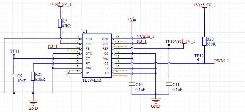
    I'm using the configuration bellow : 

    The ideia is to feed a control signal, on pin 16, between 0.7 and 3.7V to vary the Duty Cycle between the minimum ( 0% ) and the max.

    I'm having two issues with it that i cannot understand:

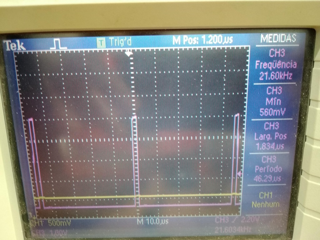
    - The PWM Frequency is 21.6kHz, when, according to the datasheet formula, it should be around 16kHz

    - Is there any way i can vary the Duty cycle from 0 to 100% ? the minimum DC is around 3%.

    - The PWM Seems to have a offset voltage of around 0.6V. Can i make the PWM go rail to rail ?

    bellow is a picture of the minimum pwm with the offset voltage

    Thanks.

    Bruno

  • Hello, 

    There is some information on the datasheet that doesnt add up. 

    On the datasheet is presented the grafic with information for the Timing resistor:

    According to this graphic, for a Frequency Around 16kHz, the resistor should be 8.5kR (?) 

    Using the formula given on the datasheet for the frequency, for a 16kHz, using a 10nF capacitor, the result is 6.25kR.

    Using the 6.2kR , as i've shown on the previous reply, the frequency is around 21k.

    Can you please clarify this point ? 

    Thank you.

  • Hi BD,

    First, apologies for the late reply.

    It looks like number 1 amp is tied low by the inputs, and amplifier 2 is configured as an voltage follower, inverting input connected to its output FB.

    Have you checked to see if the FB pin is following the VCrtlin_1 voltage as it changes?

    Note that the output stage is driven by bipolar transistors so there will be a voltage drop across the transistors when they on, a VCE sat, see page 6, section 7.8, of the datasheet for details.

    The log scales are difficult to read especially if the value does not fall on the crossing point of the major units. If the value falls midway on a log scale then the value is sqrt of 10, 3.16, not 5. Looking at the graph I would have selected a resistor value around 7k for 16kHz.

    Regards

    Peter

  • Hi BD,

    Since there has been no response to to my last post I hope that you have made some progress on this issue.

    Pleas open a new post if you have moer questions.

    Regards

    Peter

  • Hello Peter,

    Sorry for the late reply.

    I had to change the approach since the TL didn't fulfil the requirements ( i couldn't deliver a precise pwm in therms of duty cycle nor frequency ) and additional ones were asked.

    Thank you for the support.

    Best Regards,

    BD