This thread has been locked.

If you have a related question, please click the "Ask a related question" button in the top right corner. The newly created question will be automatically linked to this question.

LM5146-Q1: IC heating up to 100 degree at 12V and 15A temperature

Part Number: LM5146-Q1
Other Parts Discussed in Thread: LM5146

Hi,

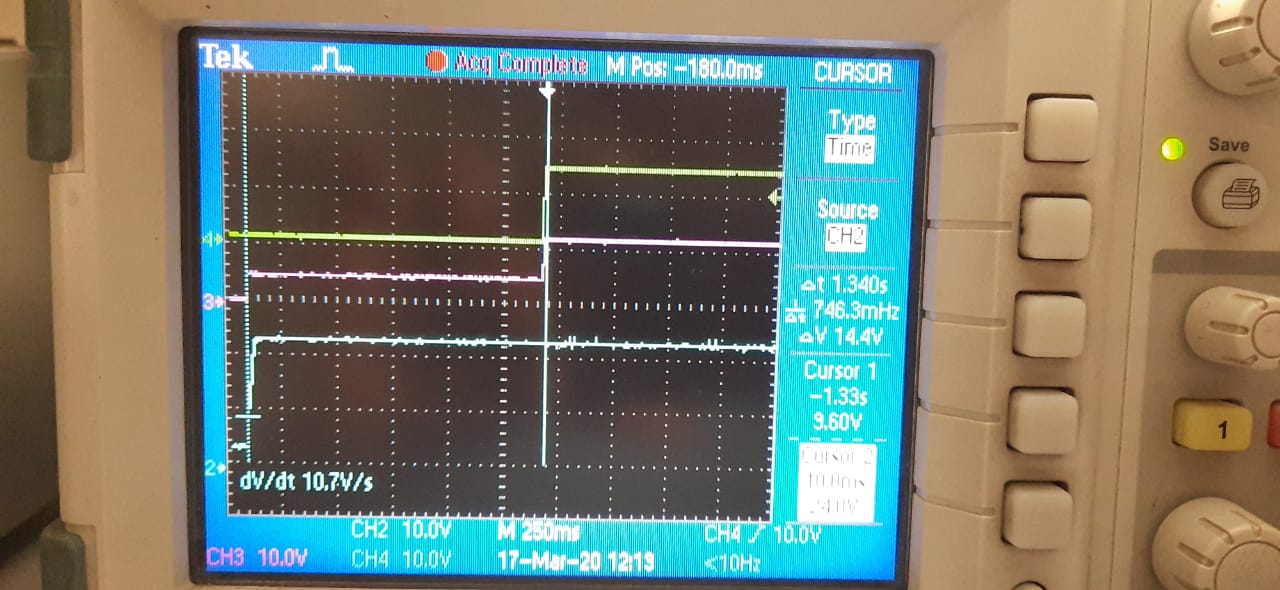
I have design DC-DC converter using LM5146-Q1, please find below input and output specifications.

A) Input voltage range: 20V - 36VDC, nominal input 24V.

B) Output : 12V / 15A.

1) at 12A load  IC is heating up-to 86 degree after 30 minutes.

2) at 15A load  IC is heating up to 100 degree.

I went through LM5146-Q1_12V-8A_EVM_TI  design and find out IC temp is 65 degree at 8A load.

I have also given VCC from output side as shown in datasheet figure 30 and also done layout as recommended in datasheet.

our schematic is as per your reference schematic.

"" can we design system up to 15A with LM5146-Q1 without forced cooling.""

we have used 2.2 ohm gate resistor, but in your reference schematic gate resistor is not used.

We need your guidance to finalize design.

Thanks and Regards,

Mahesh Kohale.

  • Hi Kohale:

    1. is the IC close to mosfet, so that the mosfet will heat up the IC.  when Io=0A, is IC hot?

    2. if Io=0A, IC still be hot. What's the mosfet Qg and fsw you choose, the IC's power dissipation is proportion to your mosfet's Qg and fsw. The drive current provide by Vcc is equal to 2*Qg*fsw. 

    for LM5146 deliver 12V 15A, it need set a low working frequency like 250Khz or even lower to reduce the switching loss. we have excel calculator you can download for efficiency and loop calculation.

    Thanks

    Daniel Li

  • Hi Daniel,

    1) we have set switching frequency =230Khz

    2) For No load condition (Io=0A) and VCC from output side not connected then IC heating, but as VCC from output connected then IC does not heat at No load.

    3) Mosfet Qg= 55nC, what is maximum Qg we can use.

    4) dead band of IC is 14ns, is it affecting while switching of Mosfet?

    5) in your reference schematic you have not connected any gate resistor ? do we also remove gate resistor.

    Thanks and regards,

    Mahesh 

  • Hi Daniel,

    we have connected SYNCIN and SYNCOUT pin to ground, is it ok? 

    In datasheet, do not found anything related to SYNCIN and SYNCOUT pin.

    Please guide us on this.

    Thanks and Regards,

    Mahesh

  • Hello Mahesh,

    Has the thermal issue been resolved? It looks like you are discussing another concern now.

    Please use datasheet as reference for selecting output FETs and considerations when balanacing rds and qG. Since thermals was a concern, to minimize loss and to minimize heat dissipation, you would want to select output drivers with minimal qG requirement, especially if switching at high frequency.

    The rise time on the gate, must be much faster than the minimum on time, dictated at high input voltage. Switching frequency can be manipulated to increase on-time,

  • Hi Marshall,

    Our heating issue has not resolved yet.

    What I have asked above about SYNCIN and SYNCOUT is regarding heating of IC.

    In Datasheet and reference circuit SYNCIN and SYNCOUT pin is not connected to ground or VCC.

    I got the point of selecting Mosfet with appropriate Qg value (as per 2*Qg* fsw ).

    Thanks and Regards,

    Mahesh Kohale

  • HI

    pls leave SYNC in and SYNC Out float if you do not use it.

    Thanks

  • Hi,

    we will make this provision in our new schematic.

    but I found in LM5146-Q1 quickstart tool as below : 

    If SYNCIN and SYNCOUT pin is not used then either ground in DCM mode or connect to VCC in CCM mode.

    Should we go with keeping both pin floating.

    Thanks and Regards,

    Mahesh Kohale

  • Hi 

    sorry for the confuse.

    Cause SYNCIN is dual function pin, if you need diode emulation mode, pls keep SYNCIN to AGND. if you need FPWM, pls tight to VCC.

    for SYNCOUT, cause I see EVM is OK with SYNCOUT floating. you can follow quick calculation tools for SYNCOUT configuration . Tie to fixed voltage(VCC or Ground) may be better.

    And from your description, i think the Qg of mofest, fsw with internal LDO is key for IC heat.  

    Thanks

    Daniel Li

  • Hi,

    As we designing DC-DC Converter with LM5146Q1, we need below details:

    1) EMI / EMC report of LM5146Q1 IC.

    2) Road map of IC.( as how many years it will be active or continue)

    Thanks and Regards,

    Mahesh Kohale

  • Hi:

    1. EMI Report, you can refer EVM user guide

    http://www.ti.com/lit/ug/snvu591/snvu591.pdf

    2.Road map of IC: For the device statues(active or EOL), you can check with our sales or Disty, as I know, Ti won't EOL device when customer need it.

    Thanks

  • Hi,

    In our going testing we are facing below issue:

    1) When we start input supply then first 4.5V VCC generated for 2 to 3 seconds and then 7.5V VCC generated,

        due to which output generated after 2 to 3 seconds. 

        what is reason for this VCC problem?

    2) If we connect output load initially then DC-DC converter do generate output as VCC is always 4.5V and do not increase to 7.5V,

       and when load decreased then it take 1 to 2 minutes to reach VCC from 4.5V to 7.5V.

    I have gone through Datasheet and application note and do not find anything related this issue.

    Please guide us on this issue.

    Thanks and Regards,

    Mahesh Kohale

  • please find waveforms for  above issue.

    Blue is input, RED is VCC which is 4.5V first and after 2 seconds it rises to 7.5V,  GREEN is output which comes after 2 second.

  • please find waveforms for  above issue.

    Blue is input, RED is VCC which is 4.5V first and after 2 seconds it rises to 7.5V,  GREEN is output which comes after 2 second.

  • Hi

    when use Vin power up internal LDO, it has limited current capability for driving mosfet. how many mosfet you used? 

  • Hi,

    we are using single Mosfet as it has limited current capability.

    but as shown in above images, problem is about VCC generation.

    as VCC is initially 4.5V and then increases gradually after 1 to 2 second to 7.5V.

    Please guide on this about VCC.

    Thanks and Regards,

    Mahesh Koahle

  • Hi

    you can remove the mosfet, let the chip work at open loop condition, see VCC has the issue or not.

    in this working conditon, you also can connect chip's SW to GND, so the drive work at no load conditon. VCC will work at early no load condition, so that you can diagnose it is mosfet issue or other issue.

    Thanks