This thread has been locked.

If you have a related question, please click the "Ask a related question" button in the top right corner. The newly created question will be automatically linked to this question.

BQ24170: Runaway current for 2-cell charging at 12V

Part Number: BQ24170

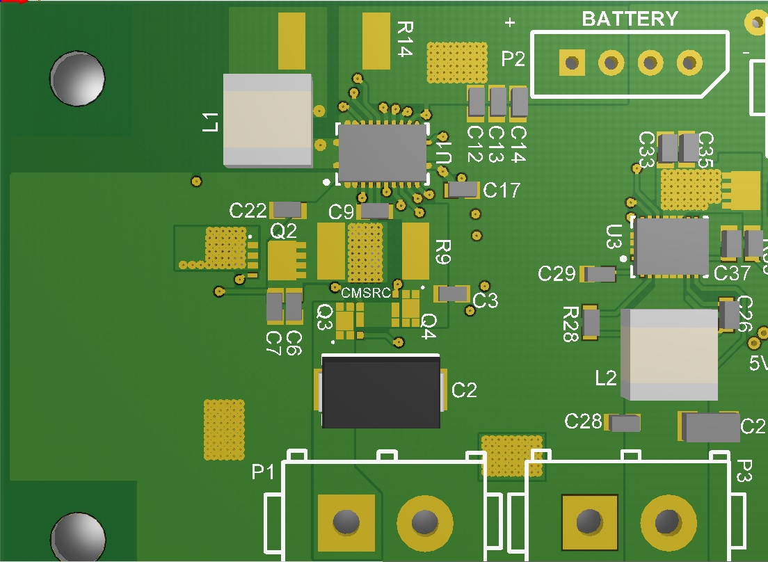
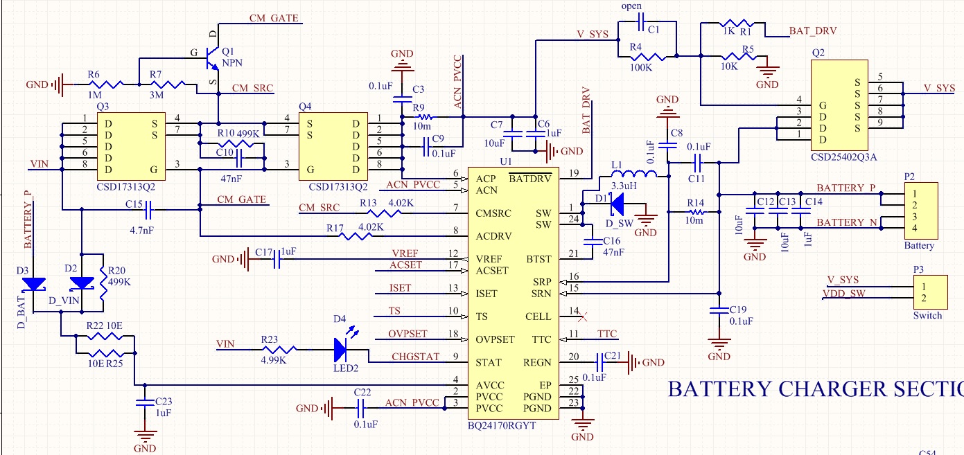
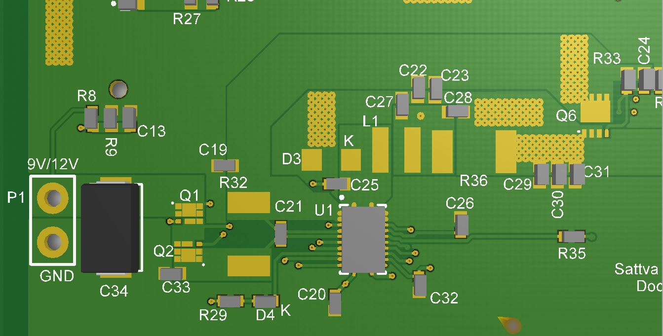
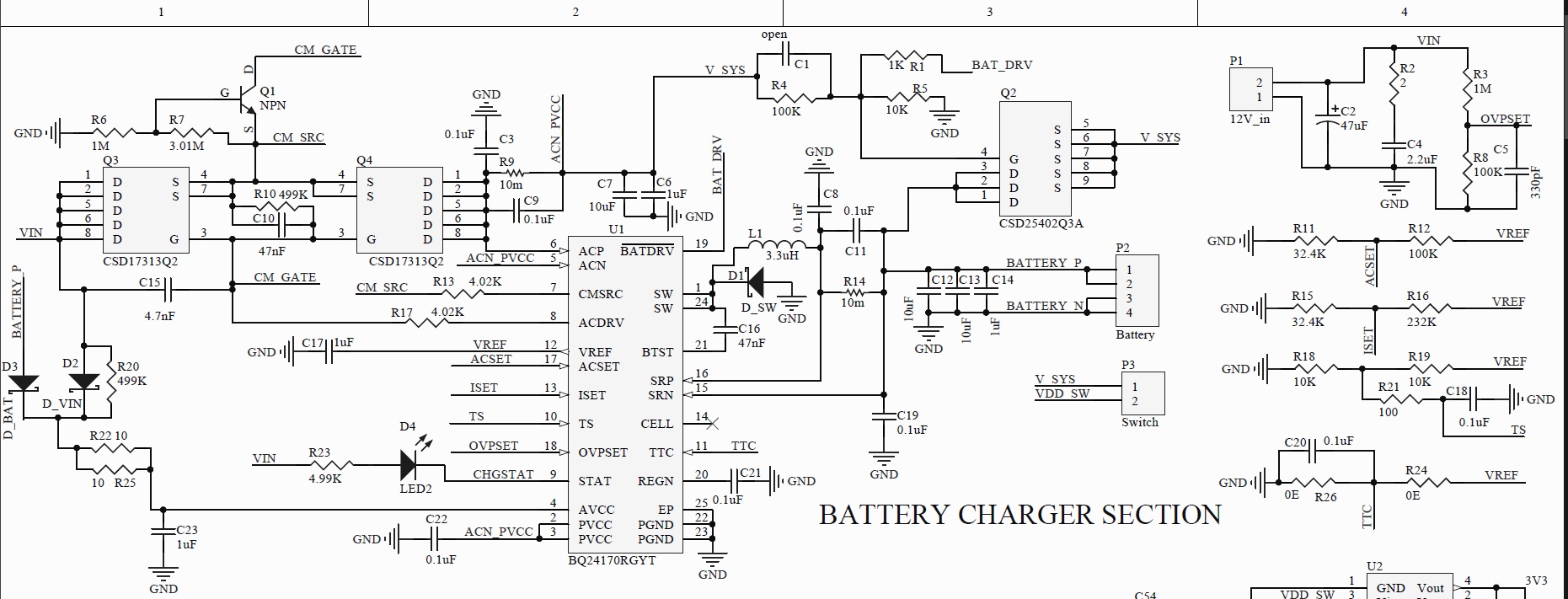
I have done two designs with this IC. Both for a 2 CELL design. Both with powered with 12V DC. Both designs have identical schematics (and the design is almost the same as the Evaluation module's schematics). However the layout is fairly different. One design works perfectly. In the second design, the battery charges perfectly if I supply 9V-11 DC. However, if I supply 12V DC, the input current gradually climbs from 1.4A to to 3A (which is the max current that my DC power supply has). The current gradually increases over a period of 5 minutes approximately and the PCB heats up to 70 degrees C, while the design that works barely crosses 45 degrees C. The components (resistors, capacitors, inductors and diodes) are identical in both designs. Clearly the issue is in the layout. I not followed all 9 layout guidelines given on page 31/41 of the datasheet in the second design. I wanted to know though: What layout flaw is the most likely cause for this gradual current rise?

  • Hi Darien,

    Just to confirm it is not the IC and is definitely the layout, are you able to move the IC from the good design to the bad design and repeat the issue?

    Regards,
    Jeff

  • Dear Darien,

    It is hard to diagnose without the layout, but I would start by seeing if you are making your traces either too narrow or too long, or a combination of both. For example, guideline 2 recommends to place the inductor input terminal as close as possible to the SW terminal, making the trace wide enough to handle the charge current. What did you significantly change from your working layout? That may be a good starting point. We do recommend following the layout guidelines in the order of precedence given in the Layout Guidelines section of the datasheet.

    Thanks,

    Mike Emanuel

    Please click "This resolved my issue" button if this post answers your question.

  • Here is what I have and have not followed from the guidelines (page 31/41 of datasheet):

    1. 10uF and 0.1uF (C7, C8 from page 18/20 of the evaluation module design) are NOT close to PVCC pin 2 and 3 of BQ24170. (A distance of about 8 mmm as compared to 2-3 mm in EVM board)

    2. My inductor is quite close to the Switching pins 1 and 24 of BQ24170. I have a 7.5 x 2 mm polygon poured over the switching pins and the switching terminal of the inductor. I am using SRP5030CA-3R3M inductor from Bourns which meets the current requirements of the design.

    3. The charging current sense resistor is very close to the Inductor. However, the sense leads are not routed on the same layer to the BQ24170. The SRN terminal is routed via the the top layer, while the SRP terminal is routed via an inner layer. I did not quite understand the 'do not route the sense leads through a high-current path'. Does this mean that I should not take these traces through the high switching current loop of the BQ24170? In the successful design though, I have routed the traces exactly as done in the EVM.

    4. The output capacitor is right next to the sensing resistor output as well as ground.

    5. I did not understand this. I have polygon poured all 4 layers in my design to PGND. (neither did I do this in my successful design)

    6. Again, I have not done this in either design. But from what I see in the EVM's design on page 14/20, PGND and AGND are connected with a big polygon on an inner layer.

    7. I have done this in both designs. 

    8. This has been done as far as possible, but to a slightly lesser extent in the second design.

    9. I have done this in both designs. 

    This is a screenshot of the not working design layout

    This is a screenshot of the schematics used in both designs:

    This is a screenshot of the working design:

    My design is in solidworks PCB which is based on Altium. But the file extensions are different from Altium. If sharing the gerbers will help, then I can do that.

  • Hi Jeff,

    Thanks for replying. Oh yes, the first design had 40 PCBs manufactured and not a single PCB had an issue. The second design had 4 PCBs manufactured for prototyping, and all 4 have the exact same issue. Could poor oven re-flowing conditions have caused this type of damage to the IC? Because the oven reflowing pattern is far from the ideal recommended curve. The temperatures do not cross 300 degrees C though. The first design was manufactured by professionals, while the second design is currently under prototype and was assembled by a small scale prototyping company. Can ESD damage cause this? (because I have learned the hard way that BQ24170 is extremely ESD sensitive) Because it works fine at 9-10V DC input. This only happens a little above 11V to 12V range. 

  • Dear Darien,

    As a first check, could you solder a known working IC to the board that is not performing as expected? I just want to eliminate the possibility that the IC is the problem.

    Second, could you please probe the ISET voltage in each case? You do not seem to bias it in your schematic. This pin along with RSR helps to set the charge current. By leaving it floating on two different layouts I suspect that the ISET voltage is different in each layout, causing unexpected results.

    Thanks,

    Mike Emanuel

    Please click "This resolved my issue" button if this post answers your question.

  • Dear Michael,

    Thanks for your response. I will solder another working IC from a reel and check and get back to you on this. Since this fault happened uniformly across all 4 assembled boards, I assumed it was a design flaw. But I will solder a working IC and check. Apologies for not posting the whole battery charging circuit. I zoomed into the IC itself and left out all voltage divider setups. Here you go:

  • Darien,

    How is the new IC working? Just wanted to see what the status was?

    Thanks,

    Mike Emanuel

  • Hi Machael,

    Sorry for the delay. I soldered a known working BQ24170 IC on this second non-working design PCB with the same effect. The current gradually rises and the board heats up to 70+ deg C. Infact I have new information. This current rise happens irrespective of 9V or 12V DC input. Earlier, I thought this happened only with 12V. We have started with a new design. We will be able to test it out in a couple of weeks. I will update you once we have tested the new design.