Hi,
I am designing a boost converter using the LM3481. When the boost converter is off, I would like the system to be in the lowest power state as possible.
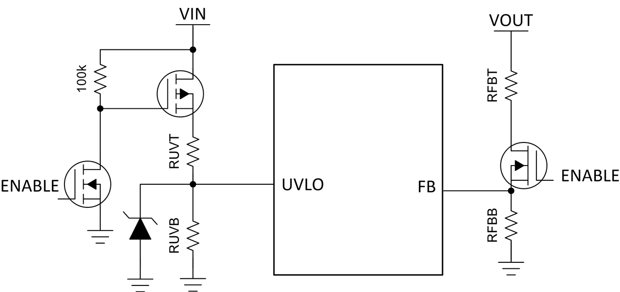
There are two resistive paths to ground:
- The resistor divider for the feedback network
- The UVLO Path to ground (with additional zener diode to prevent this pin from going >6V)
How can I reduce the current consumption of these two paths?
In a previous request, I asked for the largest resistors that can be used for the feedback network, and was told the bottom resistor should be less than 100k. For my application (Boosting to 12V), This would give a feedback network of Ra = 845k, Rb = 100k. This will limit the current to ~12.7uA when boosting to 12V. Is there a way to reduce this further? I considered adding an NMOS between Rb and ground, and connecting the gate to my Boost_En signal, but when the FET is off, the FB pin will experience >6V (though this will be through Ra). Will this be a problem if I use a FET to effectively disable the feedback network?
For the UVLO resistive path to ground, what is the maximum value of resistors I can use here to limit the current consumption? Since my VIN will be larger than 6V, I will also need to add a zener to limit the UVLO pin voltage (and this will draw additional current). I do not need to use the UVLO feature, is there a way to effectively disable this feature without needing a resistive path to ground?
Any help you can offer would be greatly appreciated.
Thanks,
Andrew


