This thread has been locked.

If you have a related question, please click the "Ask a related question" button in the top right corner. The newly created question will be automatically linked to this question.

TPS53355: power ground questions

Part Number: TPS53355

中文论坛失效,无法发帖,移步此处,怕英文描述不清,所以用中文了。

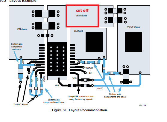
看TPS53355手册推荐layout,电源的输入电容的地,输出电容的地以及芯片功率地是连成一片的,地过孔分别靠近输入电容,输出电容,芯片功率地管脚,在功率地其他位置并没有地过孔。那么有如下几个问题

From the datasheet of TPS53355 for the recommended layout. The input capacitor ground, output capacitor ground, and chip power ground are connected together. The ground vias are close to the input capacitors, output capacitors, and chip power ground pins. There are no ground vias elsewhere in the power ground. Then there are several questions below:

1. 受PCB限制,输出滤波电容的地不能与芯片地连一起,即如图所示的地铜皮被切断了,那么会带来什么影响?

1. Limited by the PCB space, the ground of the output filter capacitors cannot be connected with the chip ground. As shown in the figure, the ground copper is cut off. What effect will it bring?

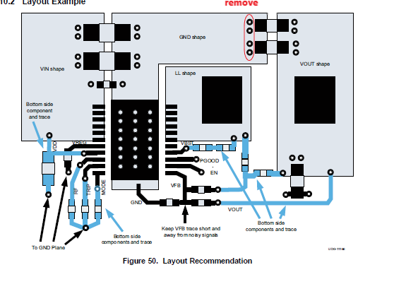
2. 受PCB限制,输出滤波电容的地过孔打不下去,所以删除了,但是输出电容的地通过铜皮与芯片功率地还是连一起的,这种情况,会有什么影响?

2. Limited by the PCB space, the ground via of the output filter capacitor cannot be punched, so it was deleted, but the ground of the output capacitors is still connected to the chip power ground through the copper skin. What will happen in this case?

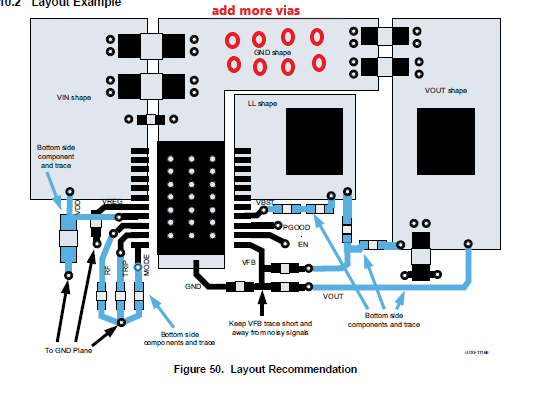
3. PCB空间足够,PCB layout工程师默认在功率地平面上增加了很多地过孔,如下图所示,增加这些地过孔有没有作用?变更好还是变更坏?

The PCB space is sufficient, and the PCB layout engineer adds a lot of ground vias to the power ground plane by default. Is the effect of adding these ground vias as shown in the figure below? For better or worse?

期待TI大佬能解惑。

Waiting for your reply!

  • 1. Limited by the PCB space, the ground of the output filter capacitors cannot be connected with the chip ground. As shown in the figure, the ground copper is cut off. What effect will it bring?

    Removing the top-layer ground return path between the output capacitors and the IC will force all of the AC ripple current for the capacitors through the vias and into internal layers.  Depending on the number of vias and the number of internal ground layers, this could increase the ground impedance and effective ESR of the output capacitors.  That will increase the output voltage ripple and the output voltage change during a load step or release.

    If the ground impedance becomes two large, it could result in an output voltage stability and regulation issue.

    High layer count PCBs with multiple ground plane layers and sufficient vias (recommend 1 via per Ampere of load current minimum) can work normally without a surface layer connection from Cout ground back to the IC power ground and rely solely on the internal ground plans to return AC switching currents PGND of the TPS53355.

    2. Limited by the PCB space, the ground via of the output filter capacitor cannot be punched, so it was deleted, but the ground of the output capacitors is still connected to the chip power ground through the copper skin. What will happen in this case?

    Removing vias in the ground area of the output capacitors will force all of the AC ripple current for the capacitors through a single top layer ground.  That will increase the ground impedance and effective ESR of the output capacitors.  That will increase the output voltage ripple and the output voltage change during a load step or release.

    If the ground impedance becomes two large, it could result in an output voltage stability and regulation issue.

    3. The PCB space is sufficient, and the PCB layout engineer adds a lot of ground vias to the power ground plane by default. Is the effect of adding these ground vias as shown in the figure below? For better or worse?

    Ideally, the ground impedance from the output capacitors back to the converter is as close to zero as possible.  Adding additional vias provides additional parallel current paths, reducing inductance and resistance and thus improving the performance.  In order to avoid adding unnecessary inductance to internal planes, is recommended that additional vias be spaced far enough apart that planes and pours on internal layers can connect between the vias. 

    Typically this requires a minimum via to via spacing of 1x Annular Ring diameter + 1x minimum trace width + 2x minimum trace to trace spacing.

  • Very helpful, thanks a lot.