This thread has been locked.

If you have a related question, please click the "Ask a related question" button in the top right corner. The newly created question will be automatically linked to this question.

LMZM33604: Track input

Part Number: LMZM33604
Other Parts Discussed in Thread: DAC53401, LM73605, LM73606

I am trying to control the output voltage of the LMZM33604 by supplying an adjustable voltage to the SS/TRK pin.  

It seems to work but I am confused by the results.  

The LMZM33604 feedback divider is set for a 3.3V output.  I expect that will set the maximum output level regardless of the TRK voltage.

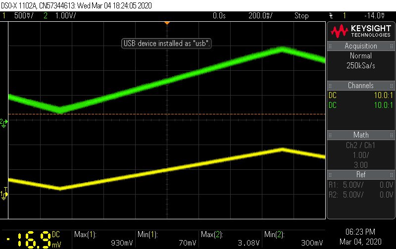
I have a DAC53401 connected to the SS/TRK pin.  It can sink the 2µA.  It can also be programmed to produce a triangle wave.  I captured the input and output waveforms.  The yellow waveform is the DAC output at .5V/div.  The green is the output of the module at 1V/div.  I put a 10Ω load across the output.

It seems to work, but the gain appears to be ~ 3.2x.  

Is that what I should expect?  I guess I anticipated a gain of 1.  The data-sheet does not suggest what the relationship should be.  Another answered question on E2E for the LM73605 controller says to expect a gain of 2.

  • Hi Barry,

    The SS/TRK pin is generally used to control how fast the output voltage ramps up during start-up with an external voltage ramp. Excess drawn input current is usually the concern when using this feature. If you care about controlling the output voltage regulation of the device, I would suggest the below:

    What I can say is that I have created a dynamic output voltage power module using a DAC injecting current into the feedback pin of the device. 

    Here is a useful app note that details the process to configure the power module for a "on-the-fly" adjustable output. In this case the more current you inject into the feedback, the lower your output voltage will be. The top resistor and the minimum injected current will define your output voltage range. If you care about fine resolution voltage steps then Rtop should be relatively small. 

    With this configuration you don't have to worry about providing an external voltage ramp. All you need here is to set the DAC to inject the desired current into the FB node which will then adjust the regulation point of the power module. I believe this is more application in your situation. 

    Let me know if you have any questions on this.

  • Thank you for the reply.  I have used current injection into feedback to control other supplies. The problem is it is non-linear which requires processing to calculate the input to output relationship, the accuracy depends on the tolerance of the resistors, and the resolution depends on which end of the non-linear range you are operating in.

    I am looking for a better solution.  That is why I am experimenting with tracking supplies.

    Do you have any data on the expected gain of the TRK input?

    It really seems this should be covered better in the data-sheet.  Tracking can also be used to ensure one ramping supply does not exceed another and you can't implement that without understanding the gain.

  • Hi Barry,

    If I were to look at your linked original question with the LM73606, Ankit is not saying that the gain is fixed at 2X. He is saying that for the customer's 2Vout, the device will track until feedback node sees 1V and then any voltage after that would not affect Vout. 

    Here is the following relationship:

    • Vout to Vfb ( set by the resistor divider ratio) 
    • Vss_track to Vfb ( 1V : 1V) 

    Using the original post reference, I took the customer's datapoints for Vtrack and Vout given a 2V output with 100k top 100k bottom resistor and plot to provide a visual below:

    Notice how Vfb (feedback voltage) tracks Vss_track up to 1V. After this 1V point, the device no longer tracks the external ramp.

    In your case I would expect the ratio between Vss_track and Vout to be (Vout : 1V). 

    Hope that answers your questions. 

    Regards,

    Jimmy 

  • After scratching my head, that does answer my question.

    The TRK gain to output depends on the Vfb divider.  I did not expect this.

    TRK has a range of 0-Vfb.  Vfb is .987-1.017 for the LMZM33604.  So the TRK range is roughly 0-1V.

    The output is scaled 0 to 100% of the resistor configured feedback for 0-1V TRK.

    Since I had my feedback configured for a 3.3V output, I got a 3.3x gain on TRK.  In the LM73606 example he had his feedback configured for a 2V output, so he got a gain of 2X.

    Now for extra points, can you explain this note in the data sheet section 7.3.13? "The external ramp final voltage after start-up must be greater than 1.5 V to avoid noise interfering with the reference voltage."

    From the analysis above, TRK is only effective in the range of 0-1V.

  • Hi Barry,

    I am trying to contact the apps engineer who has more knowledge of the core IC converter. I will relay the response when I get more information on this.

    Regards,

    Jimmy

  • Hi Barry,

    Please contact me directly at j-hua@ti.com so I can provide you with more frequent updates on your question. I am still waiting on the converter apps engineer to comment on this note in the datasheet. 

    For now I will close this thread, but please be assured I am actively pushing to get more information on this.

    Regards,

    Jimmy