This thread has been locked.

If you have a related question, please click the "Ask a related question" button in the top right corner. The newly created question will be automatically linked to this question.

TPS62140A: The reason for EOS Failure

Guru 19645 points
Part Number: TPS62140A

TPS62140A was occur EOS much for failure, please let me confirm about TPS62140A specification below;

①About TPS62140A and the same series, these device occur possibility of EOS for EN: High→Low on heavy load condition.

 ・Please let me know about threshold of "Heavy" Load.

 ・Is light load certainly not occur EOS?

 ・Is there any measure EOS for additional circuit?

②If there any correction point or confirm point for below circuit, please let me know.

Schematic and waveform, layout is attached below;

(I think that schematic was not find mistake)

Best regards,

Satoshi

  • Any update on this?

  • Satoshi-san,

    Apologies for the delayed response.

    It looks like there should not be any limit on load (heavy or light load) that should cause EOS when changing EN voltage from high to low.

    Few questions:

    1. TP1 is connected to EN. TP2 is output voltage. For the "Failure" screenshots for these test points, EN TP1 is pulled low to 0V. So, it is expected to have 0V at output (TP2). Can you please provide clear steps in the same order the test was performed? This will help us clarify what Normal and Failed operation means.

    2. Are you still able to power up your circuit and get the Normal operation working on your board?

    3. From your schematic, it looks like you are using a BJT to pull down the EN pin. Can you please confirm if the BJT is not damaged during this testing?

    4. Can you please share a high resolution pdf or image of your entire design layout? I am only able to see certain components at the moment in black and white.

    Regards,

    Amod

  • Amod-san

    Thank you for reply,

    I answer your question below;

    ①Failure IC test condition is TP1 pulled on, but Enable was not become high and 0V output.

    ②No, Failure IC is already 0V.

    ③BJT was not damage, because Failure and Normal IC were changed to connect these board.

     Results was follow around IC's specification.

    ④Sorry, customer have only these layout. 

    Best regards,

    Satoshi

  • Satoshi-san,

    Pulling the TP1 high or low should not damage the IC unless there is some other mechanism by which the IC is getting damaged. Please make sure the voltage swing on the EN pin is greater than -0.3V and lower than VIN+0.3V as per datasheet absolute max ratings table 7.1 on page 5 of datasheet. 

    Can you please share waveforms of EN pin voltage when TP1 is pulled high and low both? Please let us know the order in which you do these tests. Is the voltage violating the limits as mentioned above when the failure happens? 

    Regards,

    Amod

  • Amod-san

    Thank you for reply,

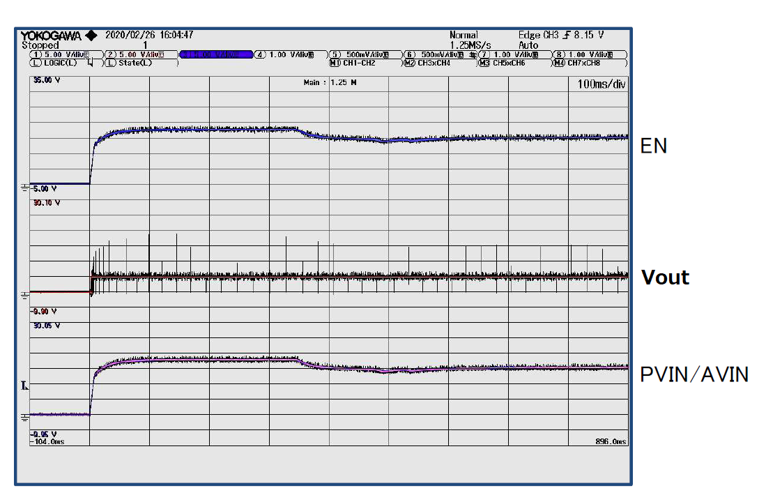
    I attached Vin and EN startup. (Both 5V/div)

    EN is startup the same timing of PVIN / AVIN, and not over absolute max rating. 

    Best regards,

    Satoshi

  • Satoshi-san,

    From your screenshots, it looks like Vout is regulating properly to 5V as expected when EN is pulled high. This looks like expected operation for the device. If you have any waveforms when the part stops working properly (transition between proper operation and failure), we might be able to look into this further.

    Regards,

    Amod