This thread has been locked.

If you have a related question, please click the "Ask a related question" button in the top right corner. The newly created question will be automatically linked to this question.

BQ76200: BQ76200 with precharge TRT and charge and discharges ways independent

Part Number: BQ76200
Other Parts Discussed in Thread: BQ78350

Hi there,

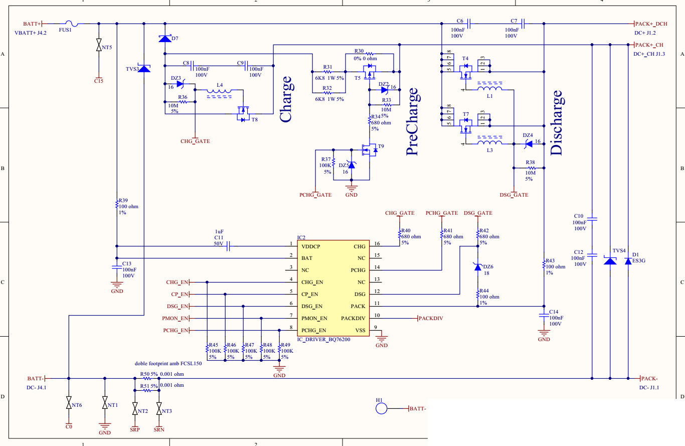
I'm working with your driver BQ76200.

On the pdf "SLVA729A–November 2015–Revised February 2016 " you can see two topologies:

- 4.1 1xCFET/1xDFET  --> Precharge transistor option with the same path to charge and discharge.

- 4.3 4xCFET/4xDFET--> No precharge transistor. Separate path for charge and discharge.

I would like to know if there is a topology with both of them features, I mean: Precharge transistor and charge and discharge path independent.

I think that this option is nor feasible because according to BQ76200 datasheet the the PREcharge voltage ON is : "V V(PACK) > 17 V, V(BAT) < V(PACK), V(PACK) – (PCHG)"  so the reference is "Vpack+". And the PACK+ pin in a precharge mode could be unknown just because they are different path.

What do you think? I'm right?

There is some option to CHG and DSG path independent; and a PRE-charge transistor, all together?

thanks a lot

  • Hi Albert,

    You are correct, the PCHG does not work on a split path schematic because it is referenced to the higher of PACK or BAT, so it would have the wrong voltage.

    You can implement a precharge feature with the same P-ch FET and resistor by adding a N-ch signal FET at GND and a dropping resistor to keep the gate voltage at an appropriate level when on. It is the voltage divider which sets the drive level for the P-ch FET. You may want a zener diode across the P-ch Vgs.  This external circuit has an advantage of allowing you to set the bias current for your needs.

    There is not an example schematic with split path and a precharge which I can recall.

  • Hi,

    I expected it. Thanks a lot.

    Mmmmmm I have done some test. Have a look to my schematic for the driver mosfet sheet and the controller.

    The DZ5 (16V) is really hot because the R41(680ohms) is extremely low. This is my fail. Beside that,

    Unsoldering the R41, I have realize that the PCHG output voltage is 50 (from Vbatt+) when is OFF; or 38V (50-12internally) when is ON.

    So, at the end my T9 (which you suggested as well) will be ON ALWAYS and the PreCahrge FET too.

    So there is no way to activate the PreCharge mosfet via BQ76200 in "separate" CHG/DSG path. You agree?

    What about that: activate the PreCharge mosfet with the BQ78350 (pin 5) /PRECHG? This pin will manage the T9 from 0V to 2,5V, and this the PreCharge Mosfet.  Even the polarity is configurable!!!

    What do you think?

  • Hi Albert,

    Right, remove the PCHG_EN signal from the input of the BQ76200 and take it to the gate of T9 removing the connection from the BQ76200 PCHG to the gate of T9 (R41).  On your board you will see how to do it best, but with R41 removed connect PCHG_EN to the top of R37.  To avoid the bias of the internal PCHG switch in the BQ76200 and since PCHG_EN seems to have a direct conneciton from IC1 pin 5 to IC2 pin 8 I expect you will have to cut the trace.  Remove R49 from the gate of the transistor, and consider making R37 much larger since it will form a voltage divider with R8.  Be sure T9 has sufficiently low Vgsth to turn on with the 2.5V level from the pull up. 

    The PCHG polarity is the same as you have been using.

    Hope this is helpful.

  • I agree.

    thanks a lot. Bravo for you