This thread has been locked.

If you have a related question, please click the "Ask a related question" button in the top right corner. The newly created question will be automatically linked to this question.

TPS63050: Diagnostic Guidance

Part Number: TPS63050

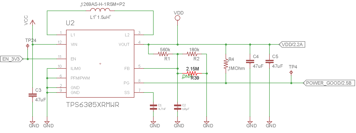
Hi, I have a TPS63050RMWR in my design and it seems to do the job. But I've got a couple of boards here in front of me that were working at one point, but not are not working, and I've traced the root cause to an unexpected voltage output from the TPS63050RMWR. I'm using the HotRod package, for what it's worth. The two boards are exhibiting incorrect behavior but in different ways. The first board measures as follows.

VIN = 4.5V

EN = 4.5V

ILM0 = GND

PFM/PWM = GND

SS = 2.32V

L1 = GND (no action)

L2 = GND (no action)

PG = GND

FB = 365mV

VOUT = 1.46V

What would you recommend doing to try and revive this board / chip? The schematic around this part looks as follows:

  • Hi Victor,

    The schematic looks fine.

    1. Did the malfunctioning board ever worked, or did they failed immediately when they were turned on for the first time?
    2. Can you please try A-B-A swap to check if the issue is not system related?
    3. Can you please share the PCB layout? You can just show the part around the TPS63050, showing all the PCB layers.

    Best regards,
    Milos

  • 1. These boards worked fine for an extended period of time befor failing (e.g. weeks).

    2. Sure I can give A-B-A swapping a go, but it's a bit challenging being leadless package.

    3. I will post local layout later, but unlikely a problem as its works,  and has passed FCC / CE testing.

  • Hi Victor,

    Sorry, I overlooked that you already wrote that the units worked initially and failed after some time. Additionally:

    1. What are the normal operating conditions in your case (input/output voltage/current)?
    2. Is it possible that the device operates under heavy loads and reaches high temperatures during normal operation?
    3. Can you please provide scope plots during startup, without a load, showing VIN, VOUT, L1, L2 and FB voltages.

    Best regards,
    Milos

  • Here's the local layout for your interest.

  • 1. Normal operating conditions are about 2.7V to 4.8V input, I would estimate peak current of 100 to 200 mA, well within the 500mA limitations of the device. Note that if I bypass the TPS63050 and supply 3.3V from an external power supply directly, the system starts up normally.

    2. The load is predictable and certainly these failures did not result from an environmental condition. They have only ever operated in my climate controlled lab / development environment.

    3. I've never heard of a scope with 5 input channels, I have one that has 4-inputs. If you had to pick 4 to see at the same time, what would they be? I don't have test points available for all those nodes either, so I'd have to tack wires onto the inductor or hole probes in place to capture those points. What are we looking in this catpure?

  • Hi Victor,

    You can split the traces over several figures, just make sure to always show VIN and VOUT, for reference. For example, one plot showing VIN, VOUT, L1, L2, and one plot showing VIN, VOUT, FB. You say L1 and L2 show no action, and yet there is some voltage on the output. We want to see the activity during startup to figure out where this voltage could come from. 

    Could it also be that you have soldering issues? Can you try reflowing the board or the device?

    As for the PCB layout, we recommend having the GND pins of the device and the GND ends of the input/output capacitors (C3, C4, C5) connected in the same layer. Check the recommended layout in the datasheet, section 11.3. I suggest connecting pins 2 and 9, and GND ends of C3-5 on the top layer, and using vias for the inductor. From the device point of view, this creates less ringing in the switching loops, otherwise the ringing might affect the device long-term reliability. 

    Best regards,
    Milos