


Hello,
I wonder why the package has more than one VIN pin configuration, not only Vin but SW and GND pin as well. Is there any specific function for this configuration? Thank you.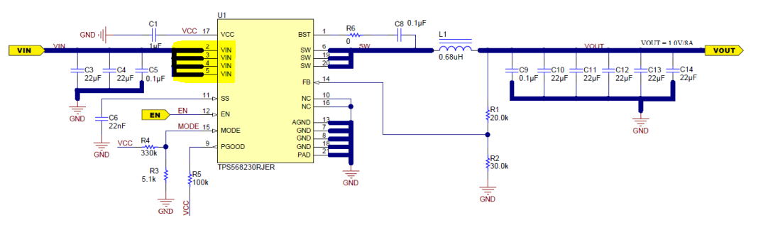
Hello,
I wonder why the package has more than one VIN pin configuration, not only Vin but SW and GND pin as well. Is there any specific function for this configuration? Thank you.

