This thread has been locked.

If you have a related question, please click the "Ask a related question" button in the top right corner. The newly created question will be automatically linked to this question.

TPS2595: Output does not recover after an output hot short to GND.

Part Number: TPS2595

Hi TI Team,

We're working with the TPS259570 eFuse in one of our systems. We encountered a strange phenomena when hot shorting the OUT pin to GND.

The device shuts down the output and latches as expected.  Our host MCU recognizes the output disconnect and toggles the EN pin to re-enable the output.

We see that the EN pin is being toggled but the output voltage is not re-enabled.

Looking at both IN and OUT pins waveforms during the short circuit, we see quite a bit of ringing. Only a device power cycle re-enables the output - EN pin toggle does not work after the output disconnect latch.

Can it be that after the short circuit and resulting voltage ringing the device enters some kind of latch-up and it's internal logic requires a power cycle? Can it be related to the internal UVP unit that samples the IN pin?

Adding input capacitance resolves this issue when input voltage ringing is reduced. I need to know if a device latch-up is possible due to input pin voltage ringing and that we really understand fixed the problem.

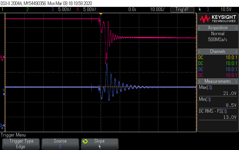
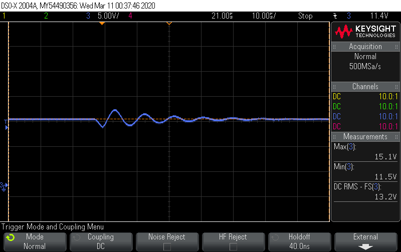
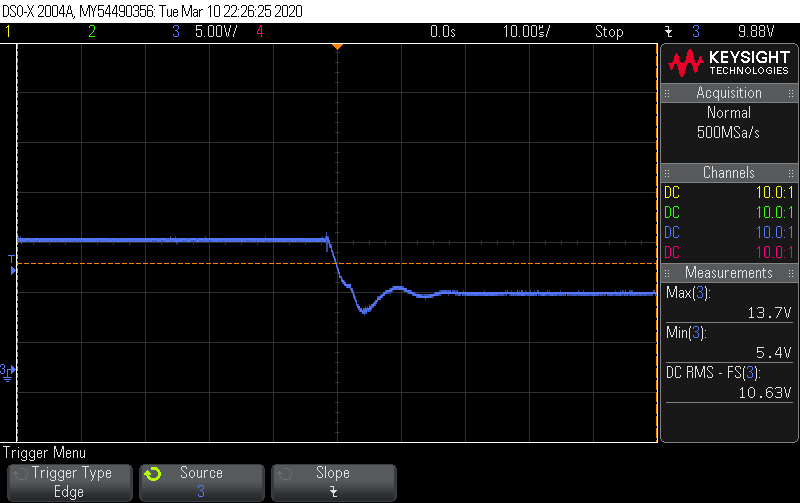
Some scope snapshots...

Input ringing with 0.1uF input cap (Blue Trace) and output ringing with 1uF output cap (Red Trace) - EN pin unresponsive, power cycle required:

Input ringing with 20uF input cap and 10uF ouput cap - EN pin is responsive and re-enables the output properly:

Output with 10uF output cap & 20uF input caps - EN pin is responsive and re-enables the output properly:

Thanks,

S.B.D

  • Hi,

    I am looking into this and will get back to you with my comments by end of today.

  • Hi,

    Can you please share your schematics with us. 

  • Hi Praveen,

    Thanks for your reply.

    Attached is a snapshot of the relevant schematics page.

    Thick red trace is a 12VDC power rail to the input of the eFuse and a small LDO.

    First scope snapshot from my original post was with C37,C17 & C24 as in the schematics.

    Second and third scope snapshot was after replacing these three capacitors to 10uF, 25V, X5R, 0603 MLCCs.

    After the capacitor change we could not recreate the problem and the device operates as expected.

    Thanks,

    S.B.D

  • Hi,

    Thanks for sharing the schematics.

    In your schematics, I don't see a TVS and Schottky diode which are placed at the input and output respectively to clamp for over voltages which can be generated during events like Fast trip /Short circuit because of the inductance present in the input and output path. 

    Over voltages which are beyond the Absolute maximum ratings of the device can damage the device. In the wave forms shared by you, I can see that the input voltage max is 21V which is beyond the Abs Max rating of 20V. Please use a TVS like SMBA13A at the input. You can refer to the TPS2595 EVM schematics for more details. 

    Can you share the waveform with all the signals captured while re-enabling the device - Vin, EN, Vout and dvdt 

    Also, what is the voltage of 12V_LP_EN signal ?


  • Hi Praveen,

    Sorry for the late reply. 
    We're currently under Corona Virus Quarantine and will be able to send it to you next week as our offices 
    are open to only a fifth of the regular workforce while all others work from home...
    As you mentioned, we also noticed the over-voltage transient on the Vin pin and also the negative voltage transient on Vout before the capacitor swap.
    Could this lead to a logic latch-up event?
    Will update you as soon as I can.
    Keep safe and healthy,
    S.B.D
  • Hi,

    Hope you are safe and healthy.

    As per design the device is expected to respond to EN signal even if there is a ringing on Vin. Have you tried replacing the IC ?

    Once you are capable of doing more tests, we can do more testing to find out the reason for this behavior. 

    As explained earlier, we recommend that you use an appropriate TVS and Schottky to make sure that the voltages at Vin and Vout are within the Abs Max ratings of the device.