Other Parts Discussed in Thread: , CSD18540Q5B
I am calculating a power budget for the power stage MOSFETs driven by an LM5170 current controller. The high-side voltage is nominally 48V and the low side varies between about 5 and 18V. I am trying to lay out a PCB and choose appropriate MOSFETs so as to ensure the design can handle the thermal load incurred by a current of 30A/phase. The design is somewhat similar to that of the LM5170-EVM, but I am hoping to avoid paralleling MOSFETs so as to create a tight power loop that minimizes ringing. More particularly, I am using the layout suggested in TI doc SLPA005 as a template for the power stage. I believe I am on the edge of what is thermally viable and, hence, want to ensure I properly understand the components of the MOSFET power dissipation... particularly the switching losses.
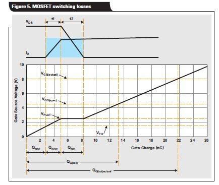
Equations (55) and (56) within the LM5170-Q1 datasheet (TI doc SNVSAQ6B) provide rise and fall time approximations that can be used in estimating the switch losses of the MOSFETs themselves (i.e., not including driver losses). Is it correct that these equations have no dependence on the gate resistance (external or MOSFET internal), i.e., that the gate driver may be considered a near-ideal current source? These equations include a gate charge termed Qg. Is this the same as the total gate charge Qg listed in a MOSFET datasheet, or is this actually only the portion of the gate charge required to fully turn on the MOSFET? Using terminology from TI MOSFETs, e.g., would this gate charge be Qg(th)+Qgs+Qgd? To take the specific example of TI's CSD18540Q5B, would the Qg used in equations (55) and (56) be Qg = 6.3 nC + 8.8 nC + 6.7 nC = 21.8 nC?


