This thread has been locked.

If you have a related question, please click the "Ask a related question" button in the top right corner. The newly created question will be automatically linked to this question.

TPS6735:

Part Number: TPS6735
Other Parts Discussed in Thread: TPS63700

Hi,

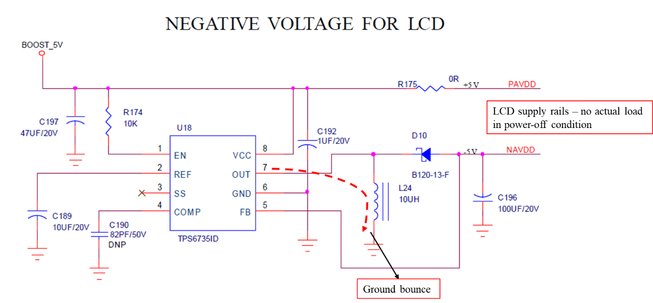
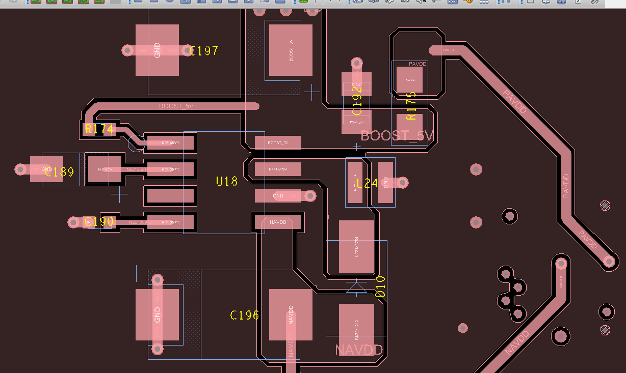
I have designed a -5V negative supply using TPS6735ID. Attached circuit image of the same.The device is battery powered. U18 input is from a Vbat to 5V boost regulator. L24 inductor specs: .

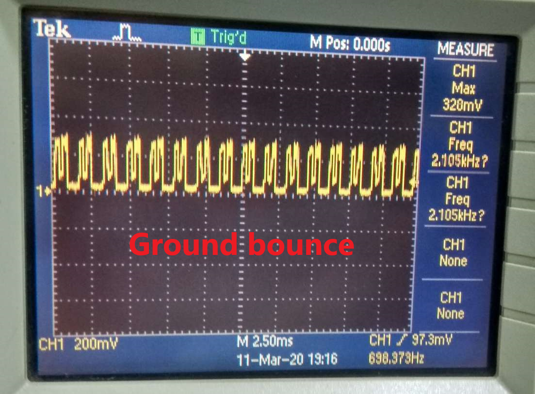
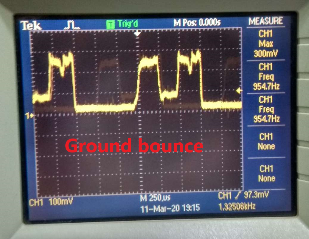
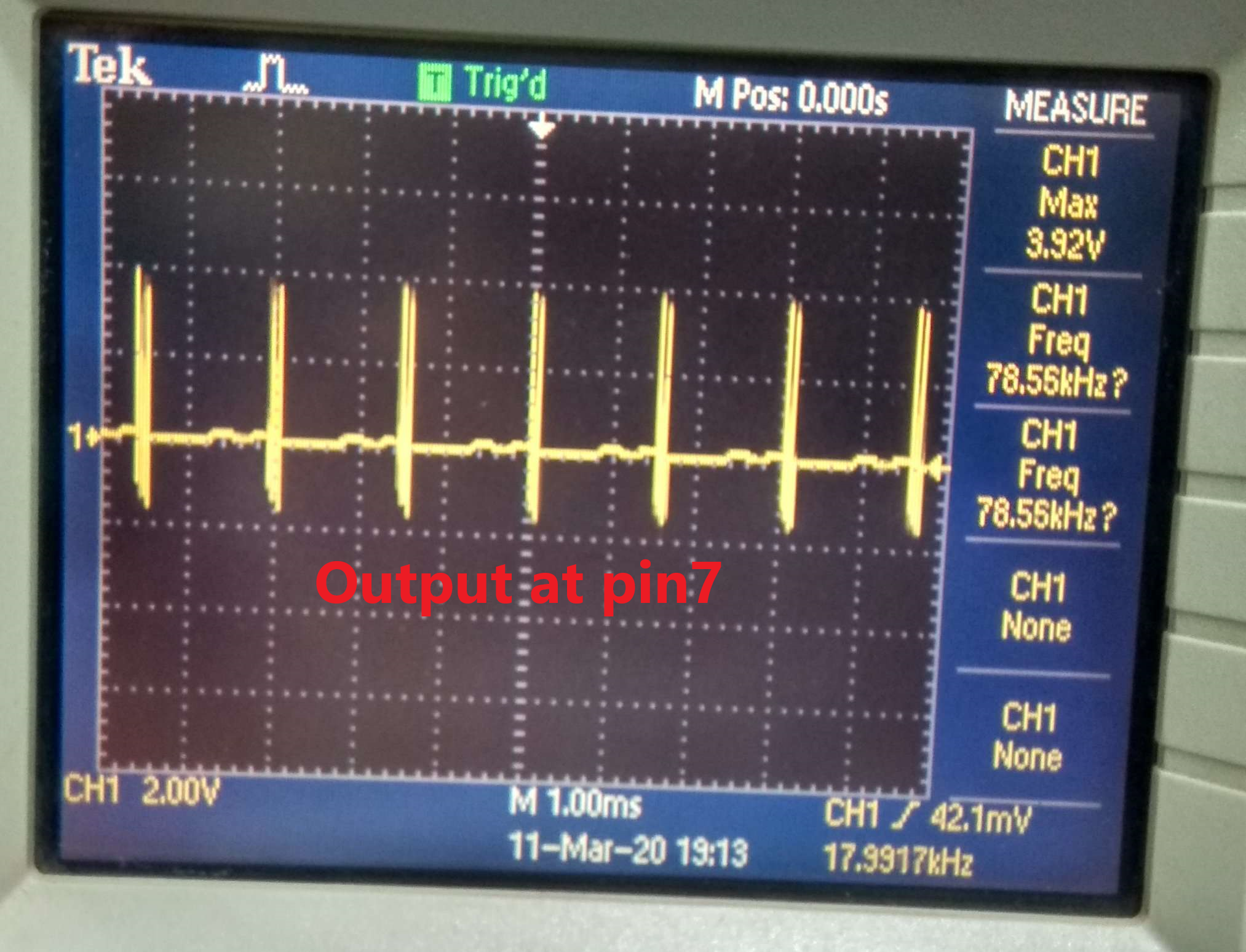
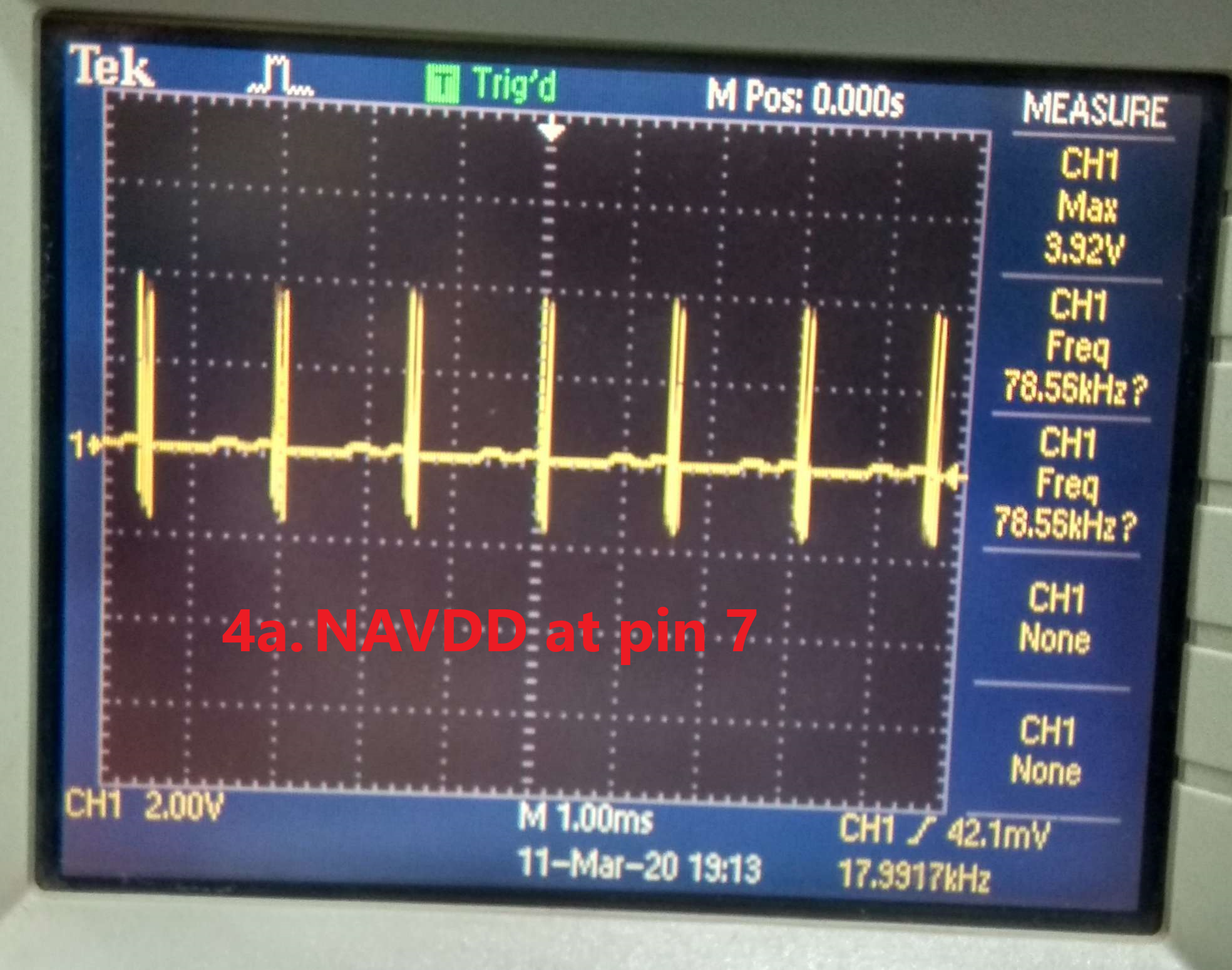
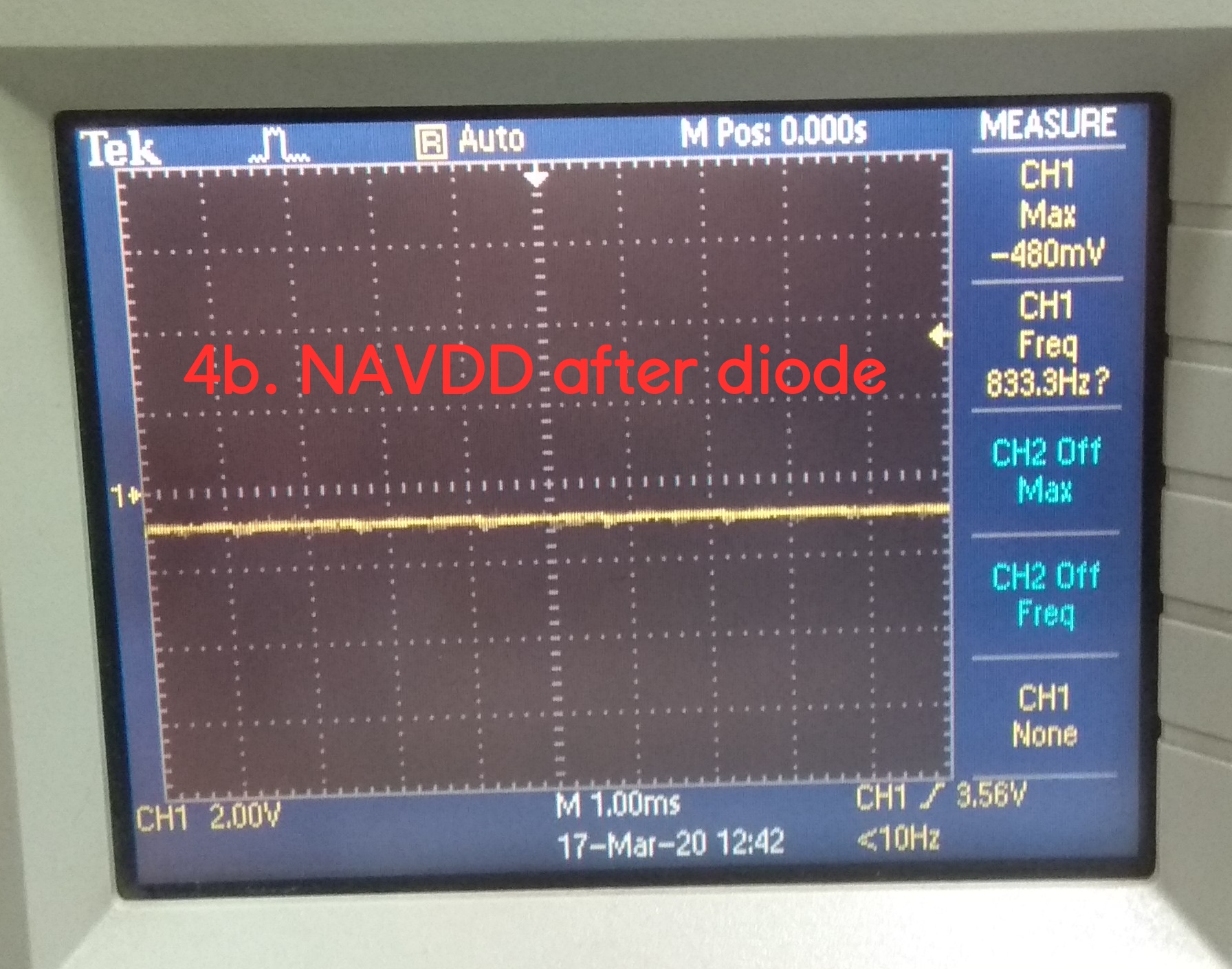
When LCD is powered on, there is an audible resonant noise from the inductor L24. When the battery is dead and charger is connected for hours, the device still shows a dead battery. When root caused this issue, it came down to TPS6735ID regulator and LCD. When the battery is dead and charging, the regulator is enabled and providing an output of 3.92V. But the LCD is not on, meaning there is no actual load for the regulator. This is causing a ground bounce at the board ground through L24. Attached images of probed signals. When this regulator section is isolated, the battery charging is stabilized and device is powering up. Is this the problem caused by the TPS6735ID regulator or the topology of my design? Please help me out here.

Thank you!


  • I missed out the inductor details.

    L24 specs: 10µH, MPN: NRS5030T100MMGJV, Isat: 2.1A

  • Hi Sumangala,

    Can you please post the PCB layout around the TPS6735? Where did you measure 3.92 V? Is the regulator generating -5 V during normal operation? The no-load input current should be around 2 mA. If this is too high, the device should be disabled via EN pin when -5 V is not needed.

    The TPS6735 is an old device, and we recommend using the TPS63700 instead.

    Best regards,
    Milos

  • Hi Milos,

    Attached PCB layout of regulator section. 3.92V was measured at output pin 7. During normal operation -4.98V is measured at output. The actual no-load (dead battery charging with LCD connected) input current is 77 mA. Is this 77 mA consumed by LCD under off condition or the regulator to ground through L24? The ground bounce is because of this? How do I rectify this without disabling the regulator (using EN)?

  • Hi Sumangala,

    Pin 7 is a switching node, you will not see a DC voltage there. Can you please summarize the output voltage NAVDD for these cases:

    1. Battery full, with the LCD connected
    2. Battery empty, with the LCD connected
    3. Battery empty, with the LCD disconnected

    Also, what is the input voltage BOOST_5V when the battery is empty and is charging? Is it still within the recommended input voltage for the TPS6735, higher than 4 V?

    I have a few remarks for the layout. The GND plane for the input capacitors and the inductor should be improved. I recommend:

    1. Move R174 trace BOOST_5V to another layer, so that it deosn't cut the GND path between the GND end of C197 and the GND pin of the TPS6735.
    2. Move C192 between U18 and C197, so that its GND end is as close as possible to GND pin of the TPS6735 and conencted through the top layer.
    3. Rotate L24 so that the GND end of L24 is right next to the GND pin of the TPS6735.

    Take a look at the recommended layout in the datasheet. GND plane is very important for switch mode converters, so try to make all GND ends of input/output capacitors and the inductor as close as possible to the GND pin of the TPS6735, and connected through the top layer, not vias. Otherwise you might have GND issues.

    Best regards,
    Milos

  • Hi Milos,

    Thank you for the inputs in layout.

    The 3.92 V is not DC but switching max 3.92 V. I had attached the probed signal in my first post. Below are the details of NAVDD.

    1. Battery full with the LCD connected = -4.97 V
    2. Battery empty with the LCD disconnected, Battery empty with the LCD connected - in both conditions NAVDD is 0 V since there is no power supply.
    3. Battery empty with the LCD disconnected and charging = -5.035 VDC, attached waveform
    4. Battery empty with the LCD connected and charging = switching 3.92 V at pin 7, 0.9 V after D10, attached waveforms
    5. Output voltage BOOST_5V when the battery is empty and is charging, without LCD = 5 VDC
    6. Output voltage BOOST_5V when the battery is empty and is charging, with LCD = 3.36 VDC

    Thank you!

  • Hi Sumangala,

    I believe you have UVLO oscillations because something before the TPS6735 is too weak to support a clean startup when LCD is connected and the battery voltage is low. Check this article for the explanation:

    http://www.ti.com/lit/an/slyt730/slyt730.pdf

    Something before the TPS6735 is to weak, causing the BOOST_5V voltage to drop when the TPS6735 turns on with the LCD connected. The BOOST_5V voltage drops under the UVLO threshold of the TPS6735 (3.7 V), and the device turns off. The BOOST_5V voltage then recovers, the device turns on and cause the voltage drop again, and the cycle repeats continuously.

    Can you connect a strong power supply instead of the battery, set it to the empty battery voltage, and connect the LCD? If you get -5 V, then the battery is too weak. If not, then the problem is in the boost converter, or connections between the battery, boost and the TPS6735.

    Best regards,
    Milos