This thread has been locked.

If you have a related question, please click the "Ask a related question" button in the top right corner. The newly created question will be automatically linked to this question.

TPS63030: Ultra-low idle current

Part Number: TPS63030
Other Parts Discussed in Thread: TPS63031

Hi,

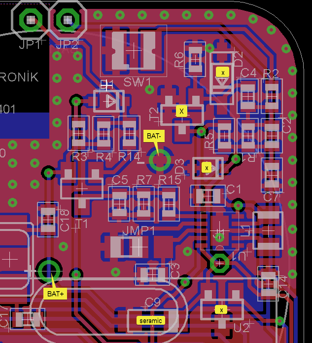
We used TPS63030 on a tracking system. The idle current (even nothing assembled on the board except power circuit) if around 4mA. We couldn't decrease it.

The board includes Atmega328p + NRF24L01 (all on board, not arduino etc). The battery is lithium 3.7V 1700mAh non-rechargeable. The device has to run in normal operation mode at least 18 months. So our device must work under 131uAh.

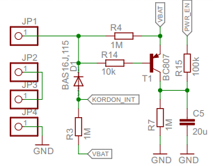
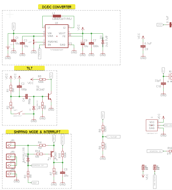
So we run MCU and RF with 1/400 duty cycle. But the idle current consumption is still too high. We enable TPS63030 with a contact based shipping mode trigger. What should we do? How can we use quiescent current feature? I suspect that the converter can wake up itself. Or what product should we use?

  • Hi Salih,

    To enable power-save mode, connect PS/SYNC pin to GND. Please refer to section 8.4.3 in the datasheet. The no-load input current should be below 50 µA in that case. When power-save mode is enabled (PS/SYNC connected to GND) the converter operates in PFM (pulse frequency modulation) mode for low output currents (approximately below 100 mA), and in PWM mode for high output currents. 

    Note that when the device operates in PFM mode, the output voltage is about 3% higher, which in your case results in around 3.4 V. This might make your D3 to conduct and cause increased input current. Also, the output voltage ripple is larger in power-save mode, up to 100 mV. This is the sacrifice to achieve high efficiency at light loads. You can also dynamically change the power mode by toggling the PS/SYNC pin during operation. For example, you can pull down PS/SYNC during standby, and switch to PWM mode when your load requires low ripple (for example during ADC conversion, data transmit etc).

    Best regards,
    Milos

  • Hi Milos,

    Thanks very much for your support. I connected PS/YSNC to the ground and put 100k (also tried 1k, 10k, 1M too) resistor to the enable pin. And I put a 10uF pol-capacitor to the output. Now the idle current goes down to the 500uA but still high. I need to go below 100uA and TPS63031 should go under 50uA as you said.

    I recorded a video about what I did. I want to be sure if I need to change IC.

    PS: Sorry, I remember wrong the IC model. It isn't TPS63030, it is TPS63031 3.3V output.

  • Hi Salih,

    Thanks for the update, I will come back to you by the end of the day.

    Best regards,
    Milos

  • Hi Salih,

    One note first. The output capacitor should really be a ceramic type. An electrolytic/tantalum capacitors have much higher ESR and ESL and are not suited for this converter. They are fine as an addition to ceramic capacitor, as a bulk storage capacitance, but at switching frequencies, they are not capacitors anymore. Additionally, make sure the output capacitor is as close as possible to VOUT, you can check the recommended PCB layout in the datasheet. You can also post your PCB layout here for review. 

    Back to your problem, can you please try removing the output TVS diode? At 3.3 V your TVS diode might already conduct a few hundreds of μA. 

    Best regards,
    Milos

  • Hi Milos,

    I took off TVS diode and tantalum capacitor. I have tried with an 10uF, 3x10uF ceramic close to the IC (parallel to the C14) and without ceramic . 100nF (C14) is already placed on the board close to the IC. Now the IDLE current is 380uA. It is getting better but still far away.

    PS: The package of the components such as C14 are 0603.

  • Hi Salih,

    I'm just double-checking, there is nothing else assembled on the board, therefore there is nothing connected to the output of the converter except for the output capacitors?

    I would try a few things:

    1. Can you try putting an inductor with a higher saturation current (and lower DCR). The one you are using is on the small side. It might happen that it saturates in PFM mode. In PFM mode the converter operates in short bursts, with the inductor current pulses typically above 200-300 mA.
    2. To get correct input current measurements, make sure you have a buffer capacitor between the power supply and the input of the converter. Check chapter 2.2 in this app note for the explanation:
      http://www.ti.com/slva236-aaj

    Also, I have a few remarks for the PCB layout:

    1. C14 should be closer to VOUT, and the GND end of C14 should be directly connected to the thermal pad. Please check the recommended layout in the datasheet, Figure 24. I can't stress enough how important the PCB layout is for a switch-mode converter.
    2. Connect the GND pin to the PGND/thermal pad directly in the top layer.
    3. C3 should be placed closer to VINA pin, but this is not that critical.

    Best regards,
    Milos

  • Hi Salih,

    Is there any update, did you manage to try my suggestions?

    Best regards.
    Milos

  • Hi Milos,

    Sorry about late response. I have just received new components for testing. I put a bigger current inductor and Iq went up to 710 uA. And also tried bigger and lower inductors as well. Nothing good news.

    Yes it is completely empty except power circuit. I decided to re-design with several chips. It is hard to fix traces on the current board.

    (DIP resistors are only for simulating the rest of the board. I have checked with and without theese resistors.)

  • Hi Salih,

    Can you please take the scope plots of Vin, Vout, L1, L2, for Iout = 0?

    And just to check, did you always use the same device, have you tried replacing the TPS63030 unit?

    Best regards,
    Milos