This thread has been locked.

If you have a related question, please click the "Ask a related question" button in the top right corner. The newly created question will be automatically linked to this question.

BQ25713: 100W Charger overheating issue

Part Number: BQ25713
Other Parts Discussed in Thread: CSD

Dear support team,

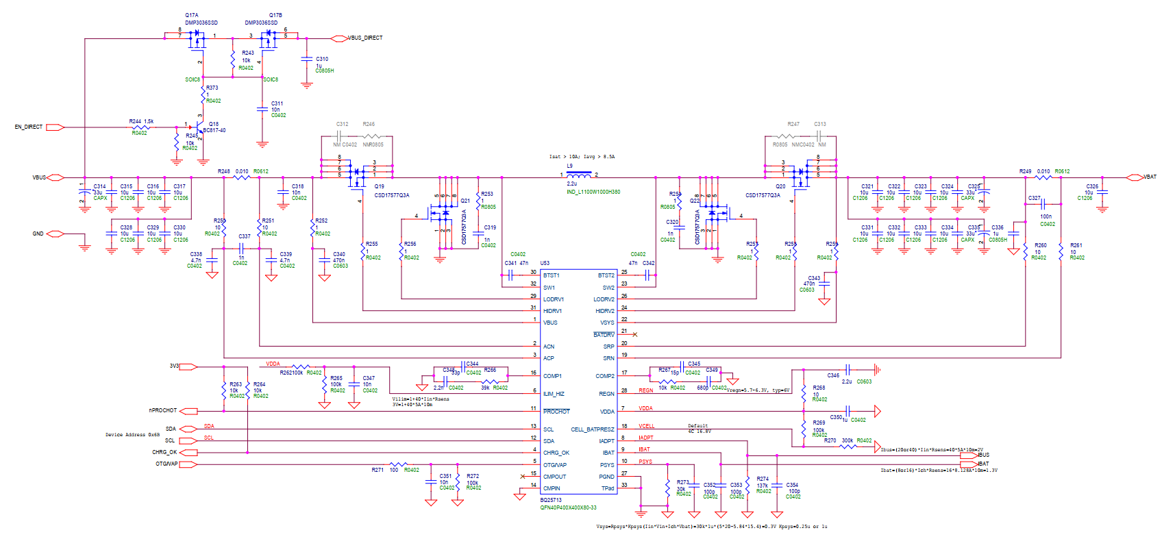
We use BQ25713 charger IC in our design.

It is used in a standard application circuit, except the BATFET absence.

4 Cell Li-Ion battery is used as a power supply. Thus, we have input power of 11.2~16.8V, 7A max.

We use CSD17577 MOSFETs and the 2.2uH inductor for the converter schematics.

Also we have RC snubbers of 1Ohm and 1nF mounted in parallel to the LO MOSFETs on both sides.

When we try delivering 100W of output power at 20V we face the overheating problem – the temperature of MOSFETs rises above 120°C, even under lightest conditions(16.8V input)

Due to the mechanical features of the design we are not allowed to use any heatsinks. Instead of them we can use MOSFETs with larger enclosure, but we are not sure whether we will benefit from that due to the high conversion frequency and increasement of the die surface.

We have already tried the next methods:

- used another MOSFETs (17304), its temperature was lower, the highest value was 126°C

- shorted gate resistors – to achieve higher dV/dt

Can you please recommend, how we can fix overheating issue? Maybe another mosfet or alternative IC?

--

Best regards,

Sergii

  • Hey Sergii,

    What are your efficiency numbers? What is the input power loss versus the output power loss?

    Can you improve heatsinking by adding a thicker layer of a GND copper pour? Can you increase the copper area of the high power traces?

    Can you reduce the effects of radiated heat by further separating the MOSFETs and inductor from each other? 

    And because you are operating in buck mode at a high duty cycle, you will likely want to consider very low RDSon MOSFETs, even at the expense higher switching losses due to a higher Qg. 

    Regards,

    Joel H

  • Hi Joel,

    thank you for the answer.

    We have measured efficiency and it is 97%. Output is 100W (20V 5A).

    Please look into SCH and layout. We have 8 Layer PCB and enough copper close to mosfets. 4 internal layers are filled with copper (2 GND shapes, 2x power shapes)

  • Hey Sergii,

    So the power loss here is about 3.1W from efficiency comment. 

    Looking at your schematic, you added 1-Ohm resistors to the gate drive signals, which will increase your switching loss by slowing down the rise time and fall times of the FETs. I would start with reducing this to 0-Ohms. This will provide some marginal improvement. I would also depopulate the RC snubbers you have added on SW1 and SW2 because these will have the same impact. 

    However, I would also mention that because you are primarily operating in forward boost mode, HSFET1 is ON a majority of the time, so it assumes the full inductor RMS current while HSFET2 and LSFET2 are switching. So selecting a HSFET with much lower RDSon will help reduce it's power dissipation significantly. Assuming you have 11.2V input @ 100W output w/97% efficiency, that is about 9A of current through the 5mOhm CSD FET you have, which equates to ~400mW power loss (about 13% of your total power loss). If you select a MOSFET with half of that, or add a parallel FET to drop this in half, it will cut your power loss by 200mW. 

    Same comment as above for the switching FETs. Reduce the RDSon as much as you can.I would also look into the reducing the inductor DCR as much as possible. I don't have information on your inductor, so I would suggest. 

    You mention 2x layers are full of copper with GND shapes. Does this mean the entire layers are all GND pours, or only some portions of the layers are GND polygons?

    As far as the layout, for one, the component designators on the layout do not match your scheamtic designators. But imagine you have the inductor on the top layer and the MOSFETs on the bottom layer. I would suggest pushing the MOSFETs further away from each other. And you may even more the inductor further to the left in order to avoid it heating the area underneath it directly, which is indirectly where the power MOSFETs are sitting.

    Keep in mind that this is mostly intuition and best guessing when it comes to optimizing the layout for better thermal performance. Unfortunately, it is very difficult to both model and simulate every possible version of component placement, PCB copper thickness, layer stackup, etc. and find the optimal layout. So I highly suggest starting with the direct power loss factors, namely the inductor and the power MOSFETs. 

    Regards,

    Joel H