This thread has been locked.

If you have a related question, please click the "Ask a related question" button in the top right corner. The newly created question will be automatically linked to this question.

UCC21222: UCC21222 Isolated Gate driver in Half bridge , how much The switch node (HS pin) can handle ??

Part Number: UCC21222
Other Parts Discussed in Thread: UCC27211, , TIDA-00364

hi 

Non isolated gate drivers such as UCC27211 can handle –18 V on HS maximum for 100 ns .

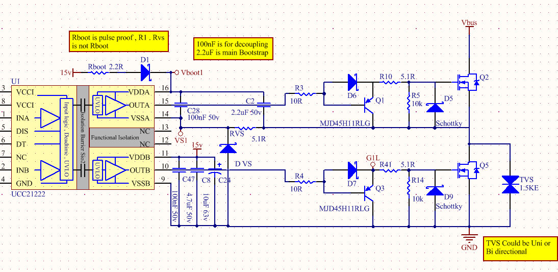
But what about isolated gate driver such as UCC21222 . when used in half bridge configuration for motor drivers (Vbus<100v).

My thought is that since there is no mention in the data sheet for the abs max rating for this pin ( VssA to VssB) . maybe it doesnot have limitation ??

1. Can you confirm my conclusion?

2. if Correct , then I should not care about reducing switch node ringing , right ?

  • Hi,

    Thank you for your question. I work on the applications team in the high power drivers group.

    UCC21222 provides two fully isolated gate drivers which are very robust to negative undershoot on the switch node and can even handle very large negative voltages due to the functional isolation between each driver.

    1. You are correct, there is no limitation on the driver for negative switch node voltage and the device can handle DC voltages down to -636V from VSSA to VDDB based on IEC creepage/clearance standards.

    That being said, it will still be important to consider the effect of negative switch node voltage on the rest of the system. If you intend to use a bootstrap supply as seen in the typical application diagram in the datasheet, it is possible to overcharge the bootstrap supply voltage which can cause violations of the gate driver abs. maximum voltage. With this in mind, it is usually best practice to either include some type of clamping circuit, like a Zener clamping diode, or to switch to an isolated power supply for the high side driver.

    2. You should still care about the effect of switch node ringing on your system and reduce it as much as possible. From my experience, switch node ringing is one of the leading causes of damage to the system if it is not mitigated. If the ringing is bad enough, we can give a variety of recommendations to help compensate, like snubbers circuits, parallel freewheeling diodes, or even updates to the actual layout to reduce loop inductance in the system.

    Please feel free to read through this app note on bootstrap circuitry selection, which still gives many good tips that can be applied to an isolated gate driver as well.

    http://www.ti.com/lit/an/slua887/slua887.pdf

    If this answered your question, could you please press the green button? If not, feel free to ask more questions.

    Thanks and best regards,

    John

  • Dear John 

    Thank u , the answer you provided was perfect .

    I do have a follow up regarding your suggestions on how to mitigate the ringing.

    According to Fairchild Ap Note: AN-6067 "Design and Application Guide of Bootstrap Circuit for High-Voltage Gate-Drive IC"

    It suggest to use a Resistor between HS pin and Switch node and use a schottky diode between Hs and Com to prevent overcharge of the C boot. 

    I updated my schematic that is based on Ti TIDA-00364 : "48-VDC Battery Powered Inverter Power Stage Reference Design for 5-kW Forklift AC Traction Motor"

    note: the schematic is showing 1 mosfet per leg , but in other variants there is up to 3 mosfet per leg. Also I will be moving to SMD mosfet to improve layout. Snubbers will not be used since they are making the ringing worse at different output currents ( load ) 

    please feel free to comment on the circuit.

    1. Does Rvs and Dvs help in making circuit more robust ?

    2. Does the TVS help ? does it have to be unidirectional ?

    3. Any other component to add to make the circuit more robust ?

  • Hi Sammy,

    I do not commonly see this technique used, but it should definitely help the bootstrap overcharge challenge. I should point out that C2 is tied to the right side of RVS which defeats the purpose of having RVS there. DVS does add some additional capacitance to the switch node as well, so it is important to consider the tradeoff between that and a different type of clamping circuit. RVS also adds additional resistance to the gate driver turn-on loop, which will potentially increase turn-on time and switching losses.

    1. RVS and DVS will probably make the circuit more robust, but they do have tradeoffs which may slightly decrease performance. This is probably worthwhile for the benefit of the system, though.
    2. I’m honestly not sure on the TVS diodes being beneficial or not since I don’t typically see them used. I would typically see an external Schottky diode to help shunt current away from the body diode of the FET while it is freewheeling. If you are using the same 100V FETs from the TIDA-00364 reference design, then they should be robust enough to handle overshoot/undershoot in a 48V system without the TVS.
    3. I might suggest adding an additional 0 Ohm resistor at the gate of the FET in case a ferrite bead needs to be added. Ferrite beads are typically useful for reducing gate ringing while hard switching at high load if necessary. I would also make sure that Vbus is adequately decoupled with the proper mix of bulk capacitance and ceramic capacitors located directly at the half-bridge FETs.

    Other than that, I have no other comments.

    If this answered your question, could you please press the green button? If not, feel free to ask more questions.

    Thanks and best regards,

    John