


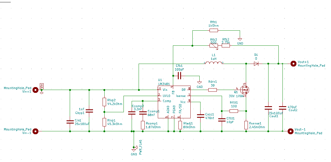
I'm making a boost converter from 3-4.2Vin to 5Vout, 10A max. Right now my test load is 12W. Schematic below
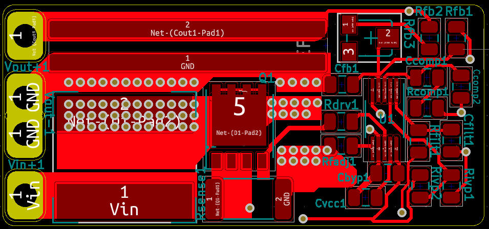
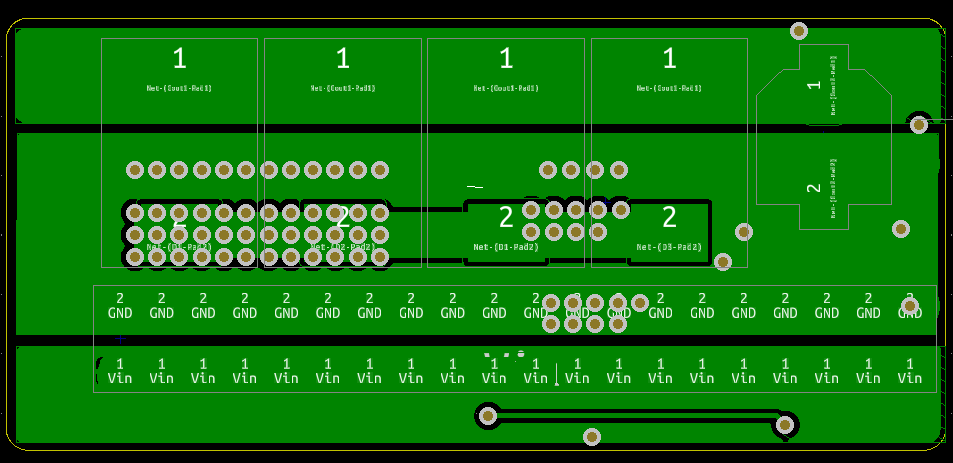
Currently, I am getting some bad ringing on the output despite having 2.5mF capacitance (mlcc). The Lower copper plane is Vin and the upper copper plane is Vout. Current flows from Vin, through the inductor, and to the copper "island" plane in the middle. Then it travels across the diodes directly to the Vout plane. I don't know if the path inductance can be reduced any further. I tried to use most direct path with shortest distance and nice big copper planes.
Here is the ringing from the output. The following was at 200mV/div and 1us/div.

This appears to be directly related to the switching mosfet. Below is the gate drive signal which is set to a frequency of 222kHz with a 15ohm gate resistor. 1V/div and 1us/div. 
Notice how the spikes in the output noise align with the rising and falling edge of the square wave. Here is another view of the output spikes in finer resolution. The following was at 200mV/div and 500ns/div:
So my question is- why is this ringing happening and how do I reduce it? I would like to shoot for a max of 20mV peak-peak output ripple.
