A related question is a question created from another question. When the related question is created, it will be automatically linked to the original question.
If you have a related question, please click the "Ask a related question" button in the top right corner. The newly created question will be automatically linked to this question.
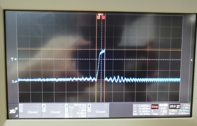
LM5106: a spike on LO pin, when device is powered on.
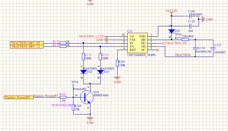
My customer's schematic is as below, they found when power on the device, there is a spike on LO pin, please help to see if there is anything wrong?thanks.
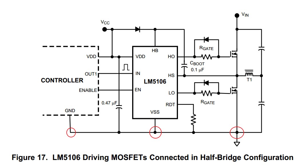
The LM5106 is a single input driver with complementary LO and HO outputs. When the IN is low, the LO will be high after the dead time of HO falling. Can you confirm the signals on IN and EN during this startup pulse? Also confirm VDD is above the UVLO threshold and does not drop below the UVLO threshold during startup.
I see on the schematic, a 1uF and 0.1uF cap on VDD and also on HB-HS. Are both capacitors populated on the HB-HS? We recommend the VDD capacitance be 10x the HB-HS capacitance so the VDD voltage does not drop significantly when the HB cap is initially charged from VDD. Can you confirm the VDD and HB capacitance values?
Thanks for the reply. I will get back to your questions tomorrow, May I have your answer about another question: is there a potential issue connecting the power stage ground with MCU ground? thanks.
The connection and routing of the grounds is importance to reduce ground bounce from the current flowing in the power stage.
Typically you want to reference, or connect the ground for the control at a quiet ground location such as the negative terminal of the power stage input filter capacitance. Avoid tapping into ground traces in the power train which are carrying high peak currents for the connection to the control circuits.
You can add some filtering in the IN and EN pins by adding some small capacitance close to the LM5106 UC pins.
Sorry for delay. I got back from them finally. It is a ground problem, they changed the LM5016 Vss from power stage side to input side, but they don't know if this is also our recommended solution for this issue. because our datasheet shows these GNDs are tied together as below. could you please also point out is there anywhere in our datasheet mentioned how to handle those different ground? thank.
It is good to hear that the problem was found to be a ground bounce, or noise issue. Can you confirm, changing the ground did solve the issue?
From a driver standpoint, for the low side driver, it is good to have the driver ground connected to the MOSFET source with a low inductance (short trace) connection. It also can cause issues if there is a lot of ground bounce from the controller ground to the driver ground, as this appears as noise/voltage spikes on the driver inputs.
Ideally the driver would be connected to the MOSFET source reference, and there is not too much ground bounce to the control ground.
Can you confirm if there is an R/C filter on the LM5106 IN pin? Place the capacitor close to the driver pins, They can try 22-50 Ohms and 100pF and not affect the delays too much. Adding the R/C filter may allow the driver connection back to the power ground.
If they still have trouble, can you provide the schematic and layout of the driver and power train, and I can make suggestions.