Hi,
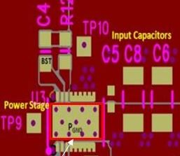
Could you tell me the recommended VIA layout dimensions on the thermal pad?
There was no description of the via size in the data sheet.
Customers want information similar to the following: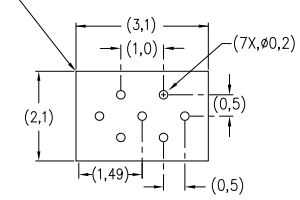
Regards,
Yusuke

-
Ask a related question
What is a related question?A related question is a question created from another question. When the related question is created, it will be automatically linked to the original question.