This thread has been locked.

If you have a related question, please click the "Ask a related question" button in the top right corner. The newly created question will be automatically linked to this question.

TPS7A85: How to minimize the output ripple noise and improve PSRR

Part Number: TPS7A85
Other Parts Discussed in Thread: TPS565208

Hi Team,

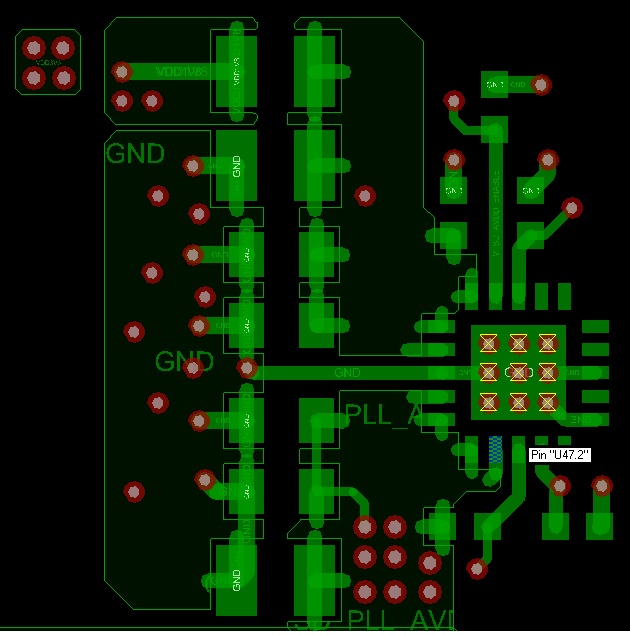
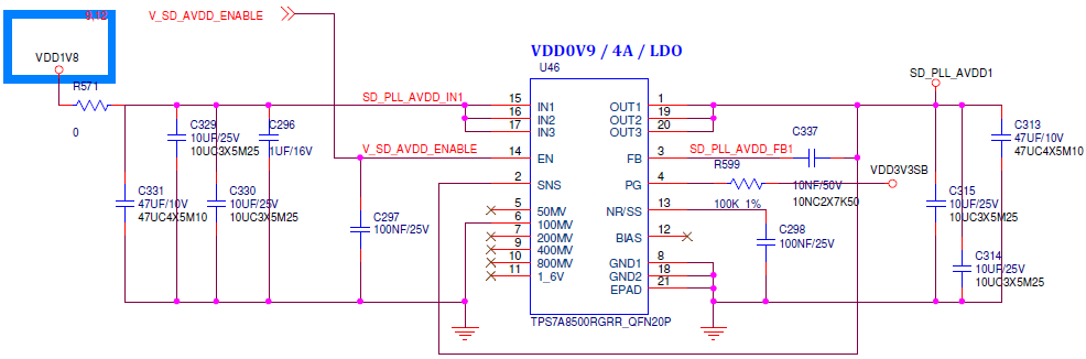
Attached is a schematic of my system design. VDD1V8 is converted from TPS565208. 

The criteria of SD_PLL_AVDD1 output voltage ripple noise is 1.2mVp-p at 600KHz-20MHz bandwidth.

I have modified the C337(Cff) to 100nF, but it does not work. Do you have any suggestions? Thank you.

Muhsiu.

  • Hi Muhsiu,

    At higher frequencies, COUT and your layout have the largest effect. See the below from our LDO Basics PSRR video

    Adding some 0.1uF and 0.01uF capacitors at the output might help. Also, the Sense pin (pin 2) can be connected closer to the load (not clear if this is happening based on the schematic).

    Also, look to see if the noise is on the ground plane. if the noise from the DC/DC converters or other switching regulators is coupling onto the GND plane, it is not possible for the LDO to filter this.  

    I hope this helps.

  • Hi John,

    Thanks for your suggestion. I will add 0.1uF /0402 MLCC at output side and measurement again. 

    The Sense pin (pin 2) is connected closer to the load as illustration below. 

    How to check the ground plane noise? Direct probing? 

    Thank you.

    Muhsiu.

  • Hi Muhsiu,

    Measuring GND noise is not easy and requires a very sensitive measurement. The point to note is that no ground plane is ideal. Like all copper traces, it has a parasitic impedance. To measure noise you have to pick a couple of GND points on the PCB and with a sensitive probe. Maybe look at GND where the power comes into the PCB and GND at the LDO. 

    Another place to look is the source of the GND noise could be the DC/C converters onboard. When looking at the input current to the converters, is there a large spike of current when transitioning from driving the low side FET to the high side FET? If so, solving this may solve the GND noise issue.

    I hope this helps.

  • Hi John,

    I had added 3 x 0.1uF/0402/16V MLCC at the output of LDO. But, it does not work. It seems to me, Due to the footprint on the PCB are 0603 and 0805. The 0.1uF can not take small ESL and ESR advantage on this PCB. I might need to have a 0402 footprint to keep ESL small. Also, the via design need to optimize to keep the current loop as small as possible. 

    BTW, thanks for another idea. [Another place to look is the source of the GND noise could be the DC/C converters onboard. When looking at the input current to the converters, is there a large spike of current when transitioning from driving the low side FET to the high side FET? If so, solving this may solve the GND noise issue.]

    If so, How to solve this large spike current? Add Rboot to reduce the turn-on speed of MOSFETs? or Add small decoupling capacitors place as close as Vin pin? 

    Thank you.

    Muhsiu.

  • HI Mushiu,

    I have had some luck in the past by either adding a resistor in series with the boot-strap cap on the DC/DC converter or if external FET's are used putting a gate resistor in the high side FET. Making sure you have Decoupling capacitors as close as possible to VIN if the DC/DC is also essential to minimize noise. 

    I hope this helps.

  • Hi John,

    Okay. Since this PCB'A including more than 10 power rails. It takes time to check them. I will press "This resolved my issue" to let you close this task. Stay healthy.

    Muhsiu.