This thread has been locked.

If you have a related question, please click the "Ask a related question" button in the top right corner. The newly created question will be automatically linked to this question.

LMZM23601: Troubles in DC/DC operation

Part Number: LMZM23601

I am using a LMZM23601V5SILT for a MCU aplication, but when i power up the DC/DC convert overheats and the Vout=Vin

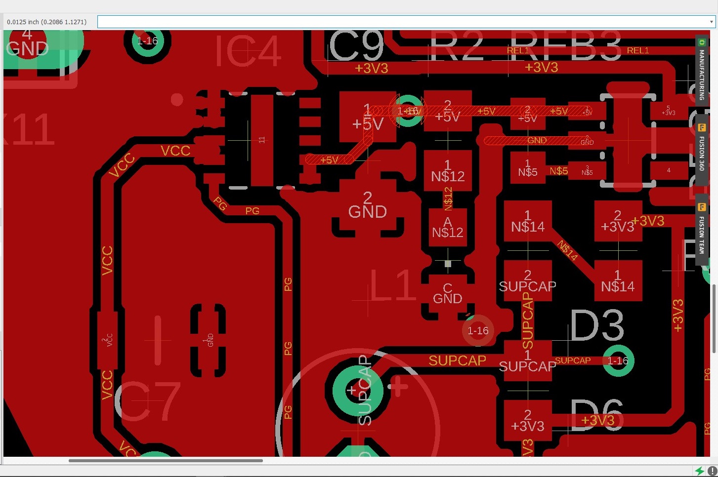
this si my pcb design

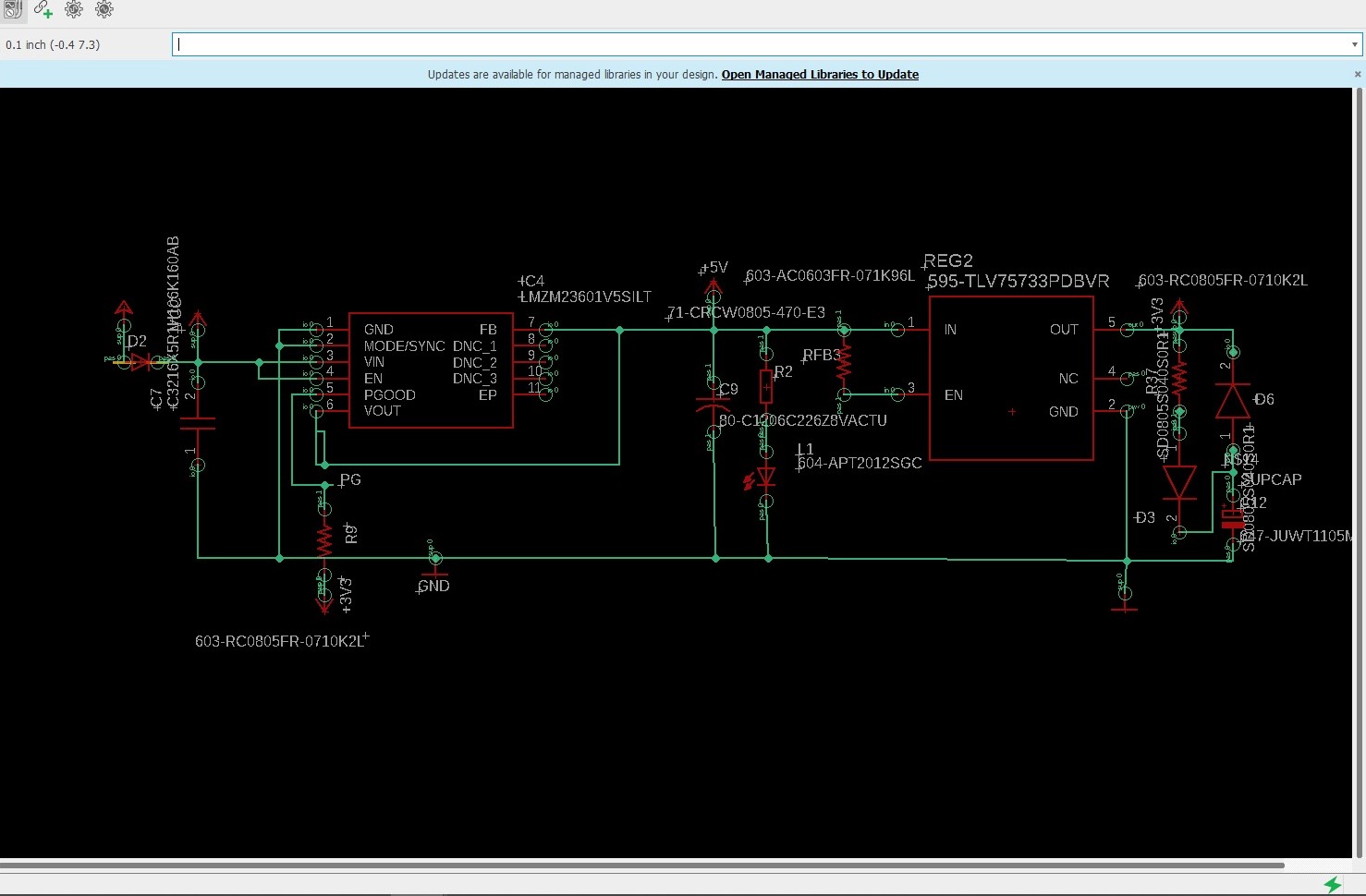
And this it the schematic

So my question 

Where wrong i am?

Coul be that thermal pad is'nt are connected to gnd 

Regards 

  • Hi Miguel,

    Can you confirm that Pad 11 is tied to net GND? From the look of the PCB layout, it doesn't look like the GND is covering PAD11. This may be the case if Pad 11 is left as NoNet. Also I would recommend you move the PG signal more to the left side parallel to the VCC trace. This way the thermal pad is not pinched to the bottom right corner of the part and heat can flow out both from top and bottom side of the power module. 

    In order to get a better understanding of your application conditions can you please comment on the following below:

    1. What is your input/output conditions? (VIN/VOUT/IOUT)?
    2. What temperature does your failure and at what stage of development (prototype, preproduction, mass production)?
    3. Can you measure continuity between each pin and ground to see if there are any shorts?
    4. Do you have a temperature measurement of the overheating condition? 
    5. How many failures are you experiencing and was the part hand-soldered onto the board or was there a controlled heat reflow?

    Regards,

    Jimmy

  • Hi Jimmy thanks

    _Yes, pad 11 dont  have connection to gnd

    1) 12 to 24 Vcd  Vin  -- 5 Vcd  Out -- Iout  150 mA, full charge, in this case we proof only with  1 LED... 50 mA or less

    2) Preproduction

    ,3) Yes but they dont have continuity 

    4)  A hand sensor :P,  we touch with finger  and the heat in component it is high 
         uncomfortable to touch  

    5) we have 1 year soldering with stencil technic and using a  

    infrared welding oven

    Regards
  • Hi Miguel,

    The thermal pad is the primary way for heat to flow out of the package. If PAD 11 is not connected to GND, this may be the reason why the part is misbehaving and overheating. Please look at both Figure 83 and Figure 84 of the datasheet. The layout guideline in Section 11.1 also suggests using a dog-bone shape copper ground for proper heat dissipation.

    Regards,

    Jimmy 

  • ok Jimmy,

    this could be make the vout=vin?.. 

  • Hi Miguel,

    The thermal pad not being connected to a large ground copper plane would result in the part entering thermal shutdown because of overheating. However this usually does not result in VOUT = VIN. In thermal shutdown both MOSFETS(High and Low) gate driver shut off until the thermal shutdown threshold limit is cleared and then the part resumes switching. Generally the waveform will look like a high output voltage followed by a pulled low voltage with some chatter before it pulls back up high.

    In your case is VOUT= VIN stable and constant? Please provide a oscilloscope image of VIN, VOUT and SW. The SW can be probed by touching the topside of the exposed inductor. Be sure to be careful when probing this since accidentally shorting SW to ground will result in a damaged part. This scope shot should help me get an understanding of how the converter is behaving.

    Usually when VOUT = VIN, there are two scenarios that come to mind. First scenario is that it is in dropout conditon where VIN voltage is low and close to VOUT. In this case the switching frequency will scale back and the output voltage will equal the input voltage with a diode drop. See Figure 4 for a graph of this condition. Second scenario is somehow the VIN and VOUT is shorted. This can either be caused by connection which you confirmed was not the case in point #3 of your reply; or if somehow the High-side MOSFET was damaged because of input voltage. Where is your 24V input supply coming from, is it a stable 24V input,  and is it possible that the input supply surged base the recommended 36V maximum rating of the VIN and damaged the part?

    In any case, I would recommend modifying the PCB layout so that PAD 11 is tied to GND for thermal relief purposes and following layout guidelines as outlined in the datasheet. 

    Regards,

    Jimmy