This thread has been locked.

If you have a related question, please click the "Ask a related question" button in the top right corner. The newly created question will be automatically linked to this question.

TPS4H160-Q1: Issue interfacing with power supply.

Part Number: TPS4H160-Q1

Hi team,

my customer is seeing failure issues trying to interface the device with the input power supply under the described condition below. please continue discussion with the customer here towards a solution.

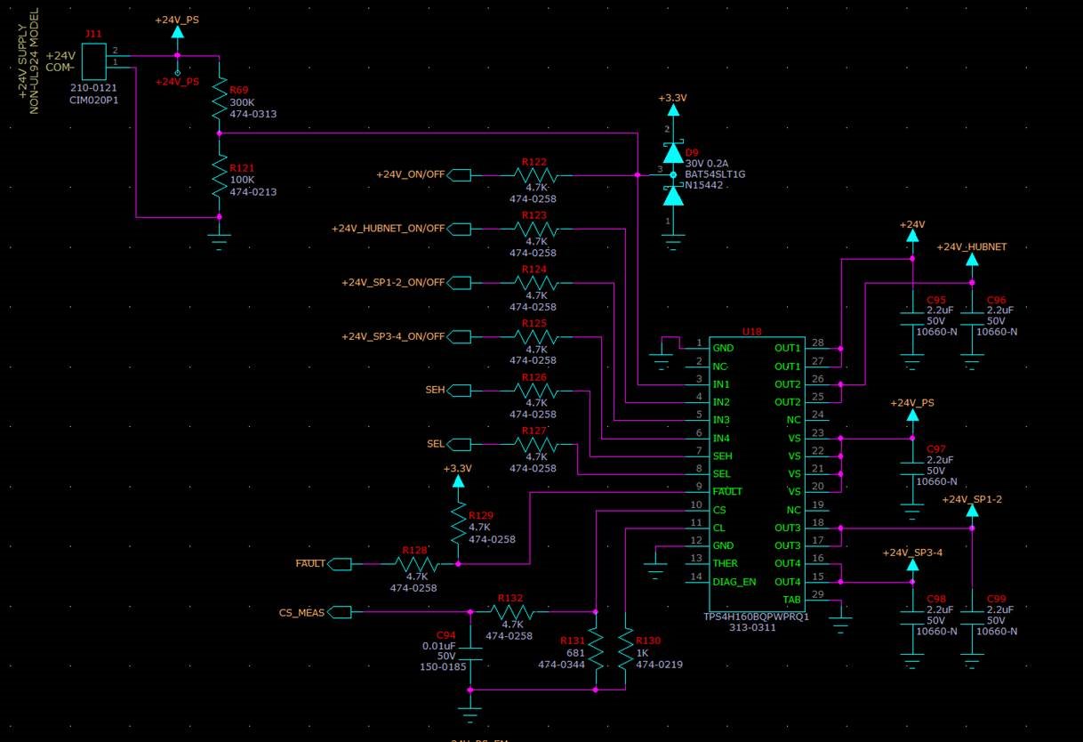
"We are using the part to enable power to different circuits. The first thing that happens is the input power enables the processor circuit that controls the rest of the loads. figure 1 shows the original schematic unchanged, We found that the diodes D9 was a problem it fed the 3.3V rail and loaded down the sense line so the switch was never enabled.

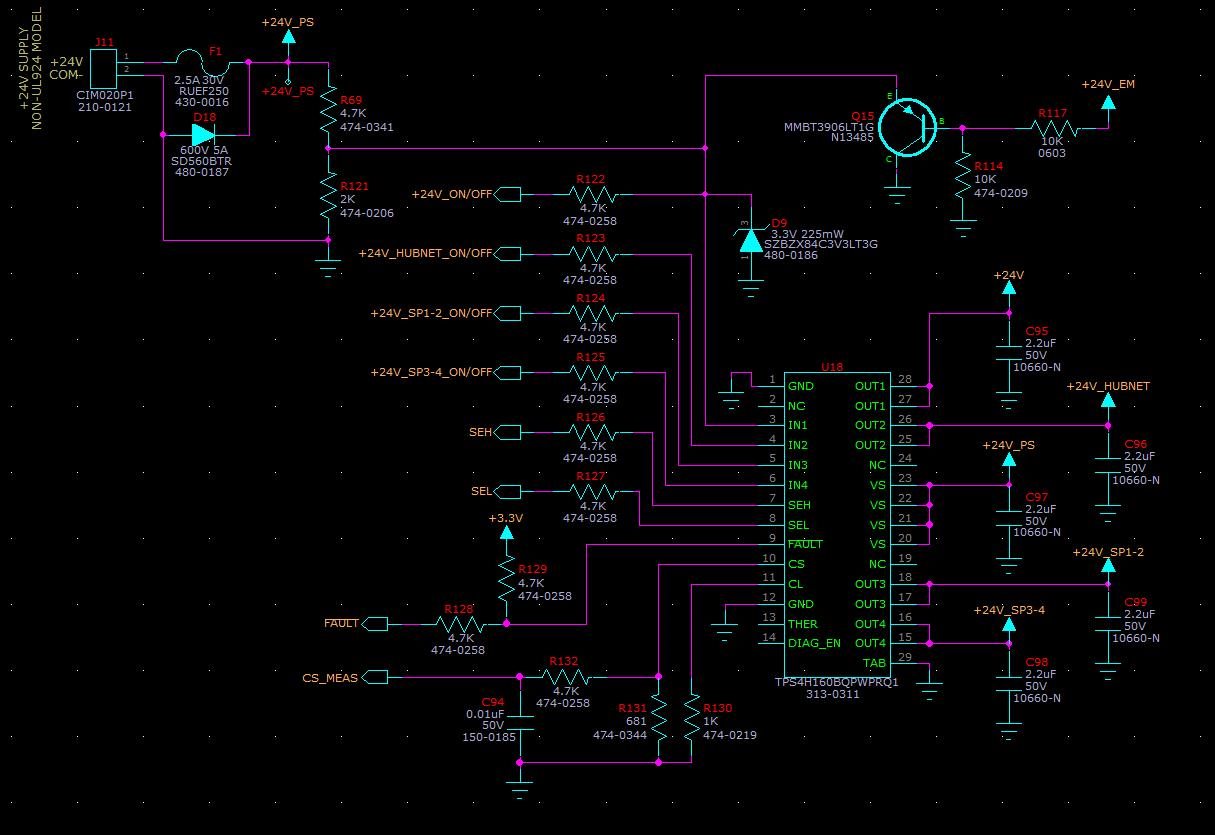
To fix this issue temporarily we removed D9 and for a more permanent fix we changed to the schematic represented in figure 2.

Currently the boards we are testing with are the units based  on the first schematic in figure 1 with D9 removed. When the 24V AC to DC supply is powered up on the AC side with the 24V out-put connected to the circuit everything operates fine. If the AC to DC supply is powered  with the 24V out-put not connected to the circuit damage will occur to the switch when the supply is connected and the 24V is already present. The AC to DC supply is maintaining regulation at 24V unloaded.

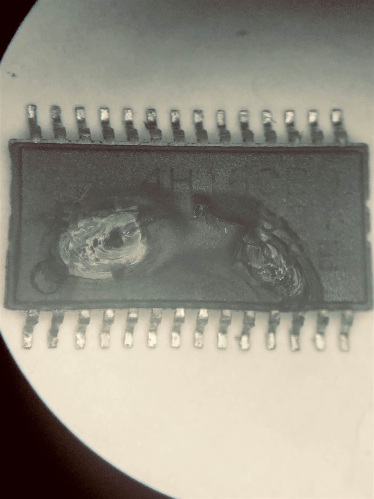
I suspect that without the over voltage protection on pin 3 there is a chance that a larger than recommended voltage would be applied and could be the issue. I am waiting for samples to test I am still interested in knowing your opinion and if this should be happening. Also I attached a picture of one of the damaged parts at the bottom of the email."

Figure 1:

Figure 2:

Figure 3:

Thanks,

Kevin

  • Kevin,

    It's hard to tell what is going on here without waveforms of power on. Do you happen to have a scope trace of the input/output signals (as well as SNS) when the device powers up?

    Also what is being driven on the load site? Are there any significant inductive/capacitive elements? What is the steady state load current?

  • Currently, the only load is on the +24V output less than 50mAs all other loads unloaded and low capacitance.

  • Thanks Tom,

    Got it- it's hard to tell what exactly is happening without scope shots, however given what you said it does seem like there is some overvoltage condition that is happening on one of the pin inputs. Something catastrophic has to happen to see the damage that you do on the IC and at a 50mA load current it's probably not some load condition as the current limit would have tripped. 

    I see in your second schematic you have that zener diode which looks to be acting as a voltage regulator for 3.3V. When the fail condition happens does that diode survive?

    Could you help me understand a little bit of what you are trying to do with the BJT/voltage divider on the IN1 line? It looks like the other IN lines are connected to an MCU/processor so I am a little unclear on what is intended to control IN1. 

    On a side (unrelated) note make sure that you have reverse polarity protection on your circuit if required. This is usually done with something like an ideal diode on the input or a resistor/diode network on the ground pin (see 8.3.7.4 Reverse-Current Protection in the datasheet). 

  • The voltage divider is there to turn on the out-put that drives the Processor power supply the transistor is to force the switch of for another condition.

    The board for the second schematic has not been ordered yet. Reverse Polarity is on the second schematic If wired backwards the input is shorted across the diode and opens the fuse.

  • Hello Tom,

    Got it- given enough of an overvoltage on the IN1 line  it is possible to damage the device as seen. The absolute max the pin is rated for is 7V. Is this an issue that is consistenly reproducible? In other words does the device always burn out as soon as the system powers up?

  • It is reproduceable we think the circuit in figure 2 will stop this from happening I just wanted to make sure I was not overlooking something.

  • Looking at the schematic everything seems in place and there is nothing striking out of the ordinary which is causing the damage you are seeing. Unless there is a significant capacitance on the load that is causing a huge inrush current or signficant inductance on the load which is causing a negative voltage spike that the TPS4H160's clamp can't handle- it is a fair assumption that overloading the control pins could cause the issue you are seeing. 

  • I am going to go ahead and close this thread. Once the new schematic comes back if there are any more issues please make a new thread (and link to this one if desired).