This thread has been locked.

If you have a related question, please click the "Ask a related question" button in the top right corner. The newly created question will be automatically linked to this question.

TPS54824: TPS54824 4.5-V to 17-V (19-V Maximum) Input, 8-A Synchronous SWIFT™ Step-Down Converter

Part Number: TPS54824
Other Parts Discussed in Thread: LM10010

Hi,

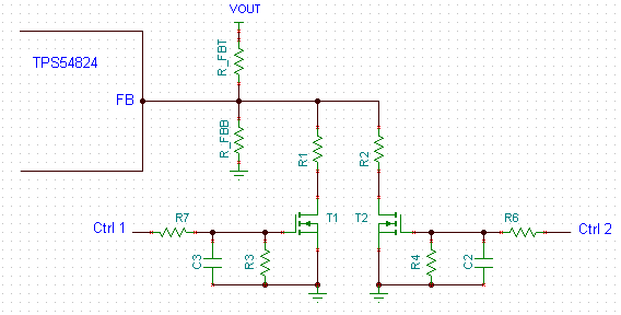
Though the Vout can be set by an external resistor voltage devider through FB (Feedback, pin 14), I like to margin Vout high / low by +/-5% as an example.  And, I'm thinking of creating passive circuits or with DAC with control signal to do that.  Wonder, is there an app notes or suggested circuit for it?

Thanks,

Tim 

  • Hi Tim,

    There are a few ways this could be achieved. First you might find the below app note useful to do this with a DAC.

    http://www.ti.com/lit/an/sbaa342a/sbaa342a.pdf

    It should also be possible to do the margining using FET switches that change the resistance in the bottom resistor of the FB divider. If this is done, I would set up the first bottom resistor to set the output voltage to -5%. One switch that adds the first resistor in parallel brings it up to 0%. Another switch that brings it up to +5%. For +5%, you could either have both switches on or just one of the switches on. If you use this method, I think you would want to be careful that they are turned on relatively slowly to avoid putting large glitches at the FB pin. I believe I have seen this transition slowed down in the past by putting a large cap on the gate of the FET. I have not tried this myself.

    Lastly, you may also want to look at the LM10010 to do this.

    Anthony

  • Hi Anthony,

    Thanks for quich response and great info!   

    the application will have many rails using this device (probably 15-20 per board), so I'm interested in using FET switches as you described as it seems to be the simplest and economical solution.   would you agree?  Do you have that circuit using FET?  

    Thanks,

    Tim

  • Hi again, 

    attached screenshot below is a sketck of my conceptual circuit using Fets, pls let me know your thought...  Thanks, Tim 

  • Hi Tim,

    That looks good. The one suggestion I have is to add an RC circuit to the gate of the FETs to give the ability to tune how quickly they turn on. I would start out with values like 1k and 100 nF.

    Also the PCB layout should be done carefully to minimize the length of trace connected to the FB pin as it is a noise sensitive high impedance node. T1, T2, R1, R2 should all be near the IC and returned to a quiet AGND.

  • One more comment. It may also be good to also have a resistor between the gate and source of T1 and T2. This way you can be sure they will stay off until the circuit has full control over the Ctrl 1 and Ctrl 2 signals.

  • Anthony,

    Thank you for quick response and great comments!

    Pls see screeshot below as just incorporated your comments.  Any comment is greatly appriciated...

    Since the FB pin is noise sensitive, if we add a small bypass caps (e.g. 100nF between FB pin and AGND as closs as possible...), would it help?

  • Looks good.

    I would not recommend adding a cap from the FB pin to ground. This can really slow down the loop response. For the FB pin 100nF is actually a very large capacitance. Small would be more like 10 pF.