This thread has been locked.

If you have a related question, please click the "Ask a related question" button in the top right corner. The newly created question will be automatically linked to this question.

TPS23523: How to invert the PowerGood pins when also using an Oring-FET?

Part Number: TPS23523
Other Parts Discussed in Thread: TINA-TI

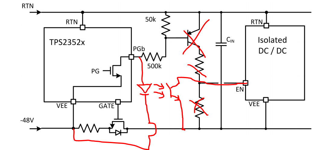
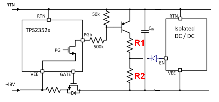
Hi, we've done a design based on the spec (9.2.2.10 Power Good Interface to Downstream DC/DC) to deactivate the downstream brick of the design.

However, we needed to tweak it a bit to get it work because we need to invert the PGb signal.

Here is what my design should have :

Hotswap GOOD
PGb = 0             Brick Enable pin = open

Hotswap NOT OK
PGb = Open      Brick Enable pin = 0

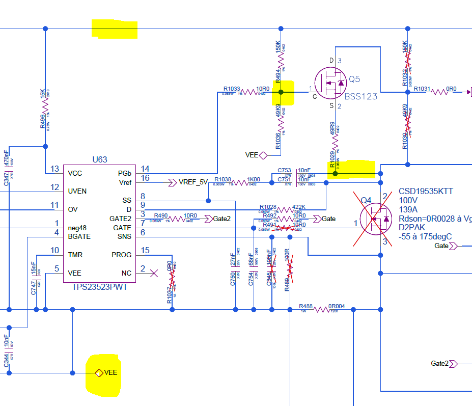
On my design the issue I just found is that the voltage divider at VEE is not working when PGb is floating because VEE became floating also because of the oring-FET!

By comparison with the hotswap spec (9.2.2.10 Power Good Interface to Downstream DC/DC)  , on my design I also have an o-ringFET on the left…which disconnect VEE so the voltage divider is no longer working between RTN and VEE…My FET is then having 48V at his gate which failed the Vgs spec of 20V and burn it I guess…

Does we can use another pin as a references to do that? like Vref or something else?

Or any other idea?

Thanks for your help!

David

TPS23523PWT_Nutaq.pdf

  • Hi David,

    Thanks for reaching out!

    The circuit mentioned in Section 9.2.2.10 Power Good Interface to Downstream DC/DC of the datasheet should work even if you use ORing-FET. Have you tried that ?

    Regards, Rakesh

  • Hi Rakesh, I didn't try the circuit in section 9.2.2.10 because on my side  it's preferable that the enable of the brick is floating instead of pullin up.  that way when PGb is floating, I need the transistor to be activated to put a 0 and deactivate the Brick instead of a pulldown, like in my schematic added.

    But by doing that VEE is disconnected to the voltage divider is not working.

    Does any other pin can serve as a reference instead of VEE?  I'm doing some calculation to use exactly like the section 9.2.2.1, but that's tricky as the brick outputs also a voltage on his enable pin when enabled...that's why it's better to make it floating to put it ON.

    Thanks

  • Hi David,

    You can consider using optocoupler as below. When PGb=OPEN, photo-diode conducts to pull down the brick enable pin to LOW. similarly, it eaves the brick enable pin OPEN if PGb=0. 

    Best Regards, Rakesh

  • Hi Rakesh, thanks for this update. This way seems similar of what I've done in my schematic

    But on my side I also have an oring FET on the "left" of VEE pin, so when PGb is floating, this FET will also be OFF and we will lost again the references of the photo-diode, like I've done in my schematic...

    If connecting it directly at -48V input, I will lost the oring-fet protection...

    That's seems difficult to find a solution…  Does the gate of the FET can be used as a reference instead? does it keeps it's references to RTN when gates are OFF?

    Thanks

  • Hi David,

    VEE of TPS2352x is the only reference available. 

    Regards, Rakesh

  • Ok, so what are my other options?  I assume that when the oring FET gate and the others FET gates are off, the chip is still alive from RTN and -48V input...so any pin referenced to RTN would work no?

    I wonder now how the OV and UVEN pins are still working when the oring-FET is deactivated thus losing the VEE connection from -Vin48? Does it takes the references from somewhere else inside the chip? (like Neg48?)

    If OV and UVEN are still good, I wonder why my schematic is not working unless there is something different internally?

    Thanks for the clarifications

  • Hi David,

    The system will have reference through the body diode of ORing FET to -48V.

    Regards, Rakesh

  • Hi David,

    Can you provide test waveforms of the highlighted nodes with respect to VEE during startup. The drain potential of the hot-swap FET varies during turn-ON and turn-OFF. As you mentioned above, this would be the reason for the FET Q5 damage.

    Best Regards, Rakesh

  • Hi Rakesh, you mean having the GND of the oscilloscope probe on VEE on the bottom or on the -48V input before the oring FET on the left? (not in the picture)

    I will try it at VEE.

    Regards,

  • Hi Rakesh, I've taken multiple screenshots, and it seems that the bug comes from the gate that is referenced to VEE, and the Source at -Vout. 

    I wonder if it would be better to reference the voltage divider of the gate to -Vout instead of VEE? like the Source pin?

    Thanks for your input

    RTN is following always the input supply, even if the voltage is below the threshold UVEN. OringFET never turn OFF?

  • Hi David,

    I have difficulty in following the waveforms as there are no labels. Can you capture something like Figure17/ Figure 18 in the datasheet with respect to VEE.

    Have you tried the optocoupler method, which was discussed above. ?

    Regards, Rakesh

  • Hi Rakesh, pictures has names that explain what they are.

    I didn't try the optocoupler version. but I guess that giving the same reference for the gate and the source would work and avoid having a VGS of 50V when OFF because of Overvoltage.

    What do you think?

    REgards,

  • Hi David,

    Sorry, I still not able to locate labels on your pictures. Can you mark on one picture or point me where it is ?

    Did you observe any GATE voltage violation for the external logic FET you added ?

    Regards, Rakesh

  • Hi Rakesh, when clicking on the picture you have the name in the address bar. but here is the ones more interesting.

    first one, the gate of the FET relative to VEE. everything seems normal.

    But the same gate, but relative to -Vout, so nearly the Vgs value of the FET, except the 50R resistor.  That where the issue is I think.  

    Hotswap Q5NP_pin1 when voltage raise above OV around 52.5V (Probe GND at VEE)

    Hotswap Q5NP_pin1 when voltage raise above OV around 52.5V (Probe GND at -Vout)

    So I try again by moving the VEE reference to -Vout, like the source of the FET, and that's working better, but not perfect.  When passing from 38V (below UVEN), to 40V (normally over UVEN), I can see the hotswap chip is trying to start, but it's blinking...when I rise more at 42V, now it works.  So it seems that maybe the FET is turning ON too fast in that way, maybe I should correct the resistors values. 

    Here is my TINA-TI simulation, the first block is the actual one, where we can see VGS issues.  The second one is the one with reference to -Vout, where VGS is better, but seems too low, I would need to validate on my setup if this is the reason it's not starting well at 40V because the FEt is not fully ON. But I think the voltage divider I add to measure the PC pin is affecting my results...how can I probe an open circuit without injecting a voltage on it?

    ThanksTinaTI_Hotswap_PG_DCDC_PC_pin_2.TSC

  • Hi David,

    Please keep us updated on your test findings.

    What is the observed VGS voltage for the external FET in your original design and then when moved to VEE ? I feel, optocoupler version would do the job. If you have components give a try and let me know.

    Regards, Rakesh

  • Hi Rakesh, I simulated your optocouler idea and it seems to work well.  I've added a supply on the EN pin to be able to measure as we want it floating, and put a voltmeter named PC even if the PC pin would be on the other side of the transistor. but that gives an idea of the behavior.

    Doing it that way, that mean we always have VEE related to RTN.  At which moment the oring FET will stop to be ON? (not in the simulation below)

    Please confirm if I understand well the behavior of the hotswap controler vs oring FET and output FET :

    1. output FET will trig OFF when UVEN or OV threshold are reached, but oring FET will stay ON
    2. when reverse connecting RTN and -Vin, all FETs will be off.

    Am I right?

    Thanks!


    TinaTI_Hotswap_PG_DCDC_PC_pin_opto.TSC

  • Hi David,

    ORing FET turns-OFF under a situation of reverse current flow through it.

    Correct, when reverse connecting RTN and -Vin, all FETs will be OFF.

    Best Regards, Rakesh

  • Hi Rakesh, thanks for this confirmation.

    About the optocoupler, I ordered some and I will give it a try surely this week.

    But I also have a concern about the robustness of that optocoupler.  What happen in case of reverse connecting, lightning surge or other non-typical input?

    Does the oring FET or others protections will be fast enough to avoid burning the optocoupler?

    Thanks

  • Hi Rakesh, I also had an answer from the brick manufacturer, do you think it will be a better idea to use that instead of the Optocoupler?   It seems less risky to way below when considering input power fails events (reverse connection, lightning surge...etc)

    What do you think?

    Thanks 

    Brick Manuf : Engineering is recommending placing a diode in series with the EN pin.  We should also make sure we don’t have an issue at turn on.  We should look at the Brick input voltage at turn on to make sure we don’t have a dip that shuts off the Brick.  We also need to make sure we have enough hysteresis

  • Hi David,

    Ok. If the above logic meets your requirement, go ahead.

    However note that the ORing FET will protect the controller, opto-coupler, end load during reverse connecting, lightning surge etc.

    Regards, Rakesh

  • Hi again Rakesh, I now testing the PGb pin like it's said in the spec, but I have issues with the activation of the PNP transistor.

    I try with what I have on hand, and I have 47K instead of 50K on the base, and 470K instead of 500K.

    But the PNP didn't seems to activate when PGb is at VEE.  When I probe the base of the PNP, sometimes it's start

    Does this design suggestion from the spec is really working as-is?  I also try to lower the 500K to 100K, it's seems to start more easily when I probe, but still need to probe the pin to make it start.

    Do you have any idea or errata on that schematic?  Would it be easier with a P-FET?

    Thanks

  • Hi David,

    At what supply voltage are you testing /  Please share part# of PNP and other resistors/schematic.

    Regards, Rakesh 

  • Hi Rakesh, I should be ON between 40V and 52V.

    On my board, I became OFF when going below 40V, and even if I'm moving the input voltage between 42 and 50V, no change, I always need to "touch" the gate to make it ON. something is borderline.

    here is my simulation with the values on board.  Transistor is the good one also MMBT3906LT1.

    Thanks for your help!

    David

    TinaTI_Hotswap_PG_DCDC_PC_pin_diode.TSC

  • Hi David,

    You mean, you need to touch the base of PNP to make it ON ? 

    The circuit is working fine in simulation. The EN voltage reaches around 4V. Are you not getting same level on hardware ? you can try by scaling all the resistor values by 10.

    8686.TinaTI_Hotswap_PG_DCDC_PC_pin_diode.TSC

  • Hi Rakesh, I know everything seems fine in simulation, but on the PNP collector, I should see around 48V when PGb is low, which is not the case, unless I try to probe the base of the PNP.  that's not taking it ON each time, but after some touch/untouch with the oscilloscope probe, that finally put the PNP ON.    I revalidated my patch and soldering each pads again to be sure, everything seems fine.

    maybe something around the base current?  I have no clue at this time...I will try again and see what could happen.

    If you have another idea, please let me know!

    Thanks

  • Hi again Rakesh, as I got no clue for the PNP solution, I tried your optocoupler one, and it seems to work as expected for under and over voltage (I didn't try reverse voltage or lightning surge).  For over voltage, when reaching around 53V, it goes OFF, and when reaching 51-52V it's coming back to life as expected.  However, when working at undervoltage, it goes off at 39V, but when trying to come back to life at 41V, hotswap is not able to start.  I see it trying periodycally, but not able to start.  When rising the voltage higher at around 45V, now it works.

    It seems to be the start-up inrush limit current but I don,t really know how to test it...the excel sheet "target inrush current" is set at 0.4A, but not not sure if is that parameter that I should change or something else. Could it be too much capacitors at the output?

    Please let me know where to begin to correct this last issue.

    Thanks

  • Hi David,

    The retry might be due to more load (>0.4A inrush current setting) at the output causing the inrush timer to timeout and reattempting the startup. 

    While recovering the Vin > 41V, what is the load ? Is your DC-DC stage enabled? 

    Can you share test waveform of Vin, GATE, Timer, input current to understand.

    Best Regards, Rakesh