This thread has been locked.

If you have a related question, please click the "Ask a related question" button in the top right corner. The newly created question will be automatically linked to this question.

UCC21750: Glitch on OUTH for second time trigger, the first time is OK

Part Number: UCC21750
Other Parts Discussed in Thread: UCC21732,

Hi Team,

UCC21750 was also used in customer for Traction inverter, and it has some issue. Could you help us on that? Thanks.

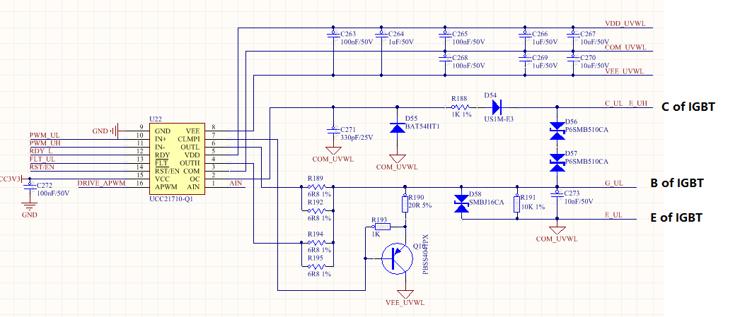
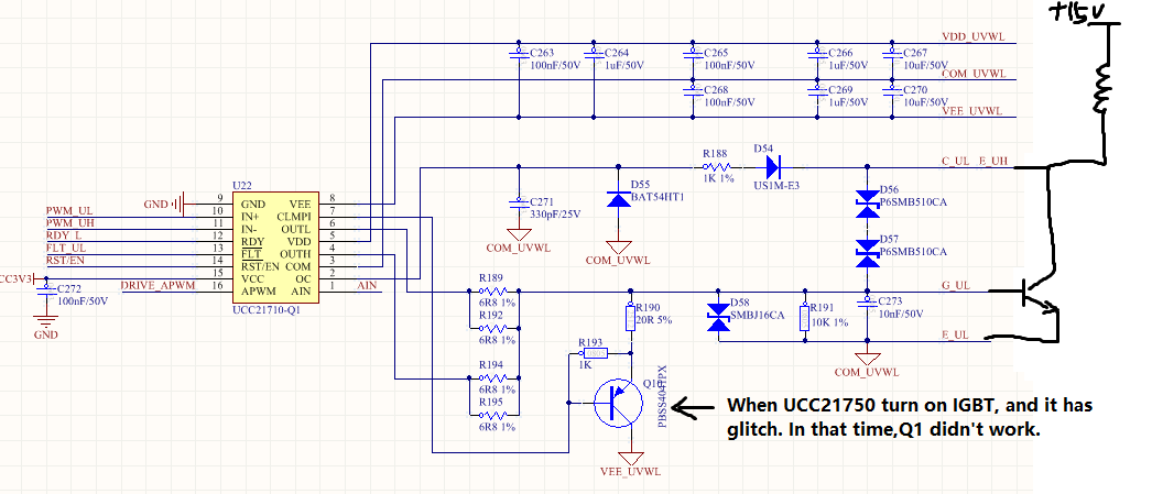
Here is the schematic from customer:

Test Condition:

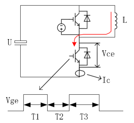
A external inductor was paralleled on high side IGBT, it shows in figure 1;

Issue:

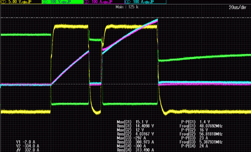
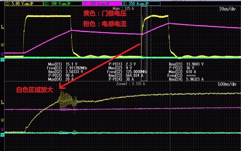
When customer used the trigger waveform to drive IGBT, it work well in T1 and T3 for the first time, it shows in figure2;

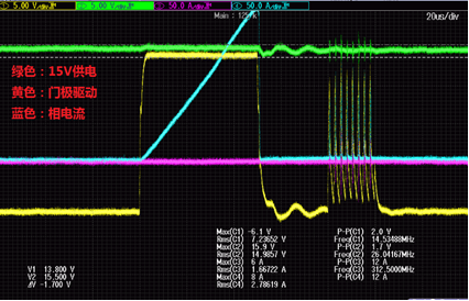
but when customer use the same waveform to trigger the IGBT for second time, it have lots of glitch in OUTH(PIN 4). It shows in figure 3.

Figure 1 Test Condition


Figure 2( Yellow for OUTH, Green for OC(pin2), Pink and blue for current in IGBT)

Figure 3( Yellow for OUTH, Green for OC(pin2), Green for 15V power of IGBT, blue for current in IGBT)

Information about IGBT

FGY160T65SPD_F085.PDF


BR

Songzhen Guo


  • Hello Songzhen,

    Thanks for all of the detailed information. I have some comments and questions:

    Did the customer change the voltage or current in the second test? Higher current or voltage results in higher transient dv/dt and di/dt. It looks like it could be an issue with shoot through. If the IGBT is not held in the off-state with a good enough pull down, then it is prone to false turn-on due to the high dv/dt transient. The Miller Clamp is used to help prevent false turn-on and keep the IGBT in the off-state during high dv/dt. This is explained here. I see the customer is using the internal Miller Clamp pin to drive an external pnp transistor. This is OK. However, there is also a 20 ohm resistor in series. This will prevent the Miller Clamp from sinking enough current to prevent the gate voltage from rising above the threshold. The Miller Clamp should have the lowest resistance possible.

    The customer should replace the 20 Ohm resistor with 0 Ohms. Or, they can directly connect CLMPI to the gate. 

    Additionally, if the customer still needs higher pull down capability, they can use a device like UCC21732 to drive a small MOSFET to be the external Miller Clamp. However, this device uses OC detection instead of DESAT, and 2-level turn off instead of soft turn off, so you will need to check with your customer what they prefer.

    The layout is also important, as the external miller clamp should be located very close to the gate of the IGBT.

    I would recommend trying to reduce the impedance of the Miller Clamp and see if this improves the test result.

    Regards,

    Audrey

  • Hi Audery,

    Thanks so much for your help.

    We try the method you recommended, but it can't solve the problem. Could you give us some suggestion on this issue? Thanks again,


    test condition Update

    High side MOSFET is disabled(Gate connect to ground), Trigger signal is used for low side MOSFET;

    The current is same for the first time and the second time.

    Issue:

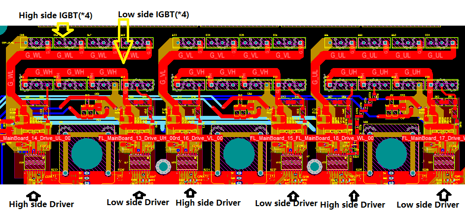
    For the low side IGBT, four IGBT were parallel connected at the same time; when we reduce the parallel IGBT to two, the glitch is disappeared.

    For parallel IGBT, three kind of IGBT were tested on customer side today. There are two kind of IGBT have glitch issue. The rest one is OK.

    Analyze

    We read the document, the issue is coursed by miller capacity. When we low side MOSFET on, the voltage on collector drop to 0V, it has a high dV/dt on collector. It can cause the error trigger on low side MOSFET.

    When we turn the Low side MOSFET for the second time, it has several glitch, but that time, the device didn't turn on Q1 to  accelerate shutdown of Low side MOSFET.


  • Hello Songzhen,

    Some other things to consider are the layout. Since there are four paralleled IGBTs, then there may be some imbalance between them. The Miller clamp should be located as close as possible to the gate, but since there are multiple gates, it is best to make it as uniform across the four as possible. In this case, the PNP should be located nearest the IGBT gate in the middle so that the IGBT closest to the gate driver and the IGBT farthest away from the gate driver are uniform. The Miller Clamp emitter should be connected directly at the IGBT gate.

    It is also best practice to use separate gate resistors for each parallel IGBT to balance the switches, as shown below:

    The slew rate dv/dt can also be adjusted during turn-on by increasing the gate resistance at OUTH. 

    Regards,

    Audrey

  • Hi Audrey,

    Thank you so much for you help.

    After co-work with customer, we reduce the length between the Base of IGBT and UCC21750-Q1. The glitch become better. But it also have a small glitch.

    There is a  thing that: customer use the same circuit to drive high side IGBT, the IGBT is also same, but it' s OK for High side part.

    Could you give some advice on the layout?Thanks.

    Here is the waveform for four IGBT after we reduce the length, the glitch become better.

    Here is the layout from customer:

    BR

    Songzhen Guo

  • Hi, Songzhen,

    Our office is closed for a US holiday.

    Audrey will respond on Monday when our office is open.

  • Hi Songzhen,

    Gate-to-emitter path from driver to IGBT should be made as short as possible. The emitter plane which connects to COM of the gate driver may be connected to each paralleled IGBT in order to ensure a small loop for all IGBTs. From the attached image, it looks as though only one emitter is connected. I would recommend connecting all emitters to the return plane and to make this connection symmetrical for all IGBTs to prevent unbalance. Additionally, it is still recommended to use a separate gate resistor for each paralleled IGBT. Each resistor should be located close to the gate of each IGBT to help dampen oscillations.

    Additionally, it should be ensured that there is no overlapping signals between the high-side and low-side drivers, especially the high-side emitter and low-side emitter.From the layout image, it looks like this was accomplished. Additional layout tips are given in Section 11.1 in the datasheet.

    Regards,

    Audrey