This thread has been locked.

If you have a related question, please click the "Ask a related question" button in the top right corner. The newly created question will be automatically linked to this question.

TPS65400: Error Amplifier Gain-BW

Part Number: TPS65400

What is the Unity Gain Bandwidth of the internal error amplifiers for this device? The data sheet does not specify. and I suspect we might be BW limiting with higher Rcomp values.

  • Hi, Kurt 

    The internal error amplifier is OTA, the trans-conductance amplifier, the GBW = Gm/Ccomp, it is related with compensation capacitor at COMPx pin. (Its own capacitance at COMPx is very small, it is about 10pF, it can be ignored.)     

  • Thank you for the rapid response Zhao Ma as I am working a time-critical problem.

    For that theoretical equation is the result in radians or Hz? And what does it typically measure on a real device?

    On the actual part I am seeing much less than theoretical even with no Chf cap.

  • Hi, Kurt 

    1. The unit is radians. 

    2. Just for OTA itself, usually it is a single pole system, so the GBW=Gm/Cc is to calculate the bandwidth for OTA itself. 

    For the buck converter system, there are other poles and zeros, the bandwidth of converter cannot be calculated by this equation.

    And you can refer the calculation in page 24 of datasheet: Feedback Compensation. 

    Usually we don't care about the OTA's GBW, we care about the whole system stability, so usually we should measure the Bode plot for the whole buck converter system. 

    3. What is the " Chf cap"? 

  • Thanks Zhao Ma,

    This is not my first time working with SMPS stability; I am very familiar with the topic. We measured the loop response of our design and found we couldn't get our desired crossover frequency. When I looked at why, it appeared as if the OTA may have insufficient BW. So I want to verify my hypothesis. 

    To answer your last question, what I call Chf is what figure 17 in the data sheet calls Croll.

    2.)  GBW for an ideal OTA is Gm/Ccomp but the OTA inside the TPS65400 is not ideal. You said there is about 10pF of stray capacitance on the COMP pin. So using your numbers the GBW should be (120uA/10pF)/(2*pi) = 1.9MHz. But there is no way this OTA has 1.9MHz of bandwidth.

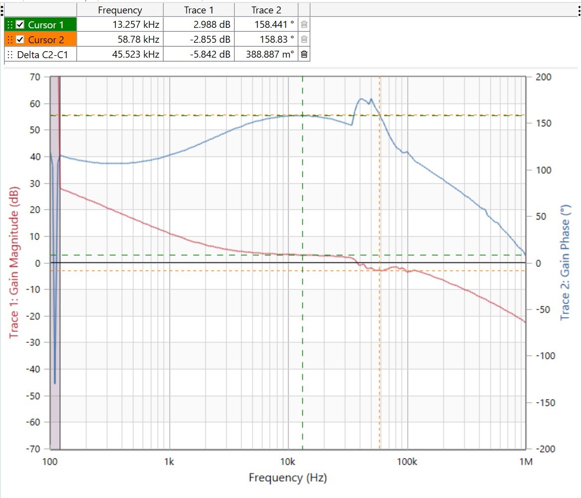
    I measured the error amplifier response  on the EVM (from TP2 to the COMP pin) with the mid-band gain set near 0db (Rc=15.4k and Cc=4700pF) with Croll=0 (not loaded.) I got the response shown below. You can see that with only the 10pF stray on COMP the OTA is already rolling off at 60kHz (-3dB point.)

    So my original question: what is the GBW of the OTA inside the TPS65400 with 10pF Cc?  Or asked a different way, what is Gm(f)? Gm has to have some dependency on frequency.

    A related question: What is the output resistance (Rea measured from COMP to ground) for the OTA? This will tell me what the open loop gain of the OTA is at DC.

    The reason this is important is we are using the TPS65400 to develop 1.1V @ 1.5A from a 12V input with very high output capacitance (200-400uF).  The switching frequency is 600kHz with a 6.8uH inductor. In this case we need to get more than 20dB of mid-band gain that is flat out to about 150kHz to be able to get the crossover frequency up to 1/10th of Fsw. But it looks like the OTA is running out of BW down near 60kHz. To make matters worse, I can't use the type 3 cap (C1 in figure 17) to counteract the rolloff because the step-down ratio is high. The zero created by C1 is passive so I can't even get 3dB out of it before it flattens out.

    I have a few other observations and questions but let's start with the OTA BW first. Thank you for as rapid a reply as you can give.

  • Hi, Kurt 

    1. As i know, there is no limitation for OTA's GBW in TPS65400. 

    Just only for OTA, usually Cstray comes from the parasitic capacitance at output node of OTA, the Cstray is not big, usually it is about 10pF ~ 30pF. The output impedance of OTA (Rea) is usually about 1Meg~30Megohm. 

    Since there are other poles in OTA itself, we cannot use Gm/Cstray to calculate the GBW for OTA itself.  

    We can use this equation to calculate the GBW only for single pole system. 

    2. What is your configuration when testing Bode plot? did you remove the Ccomp (4.7nF)? 

    From your bode plot, apparently there is a dominant pole in low-band, it looks like you didn't remove the Ccomp, did you? 

    3. I think GBW of the OTA itself inside is bigger than 200kHz. 

    Usually we can think Gm doesn't depend on frequency, it is almost fixed at steady state. 

    4. For the whole converter system in TPS65400, we usually set the GBW to ~50KHz, you cannot get flat mid-band gain to 150kHz. And you can use type 3 cap(C1) to enlarge GBW slightly. 

    BTW, 

    I am not a designer for this part, i cannot get these specific parameters. 

    Suggest to test the Bode plot for whole converter system directly, and check the pole and zero location. 

  • Hello Zhao Ma,

    You stated, "1. As i know, there is no limitation for OTA's GBW in TPS65400." If this was true then you would never say in point 4 below that "you cannot get flat mid-band gain to 150kHz," because if the GBW of just the OTA was not limited we most certainly could get flat gain to 150kHz. Way beyond 150kHz in fact.

    You stated, "Since there are other poles in OTA itself, we cannot use Gm/Cstray to calculate the GBW for OTA itself." If there are other poles inside the OTA these will limit the GBW of the OTA. You said it was not limited but now say there are poles in the OTA and poles by definition will limit the BW. This is contradictory. As I have been saying from the start, the OTA does have limited BW. You can see it in the transfer function measurement I posted above. Cstray will limit it as will the physical limits of the silicon. All I was asking is, what is the internal limit? 

    You asked, "2. What is your configuration when testing Bode plot? did you remove the Ccomp (4.7nF)? From your bode plot, apparently there is a dominant pole in low-band, it looks like you didn't remove the Ccomp, did you?" That is a plot of just the Error Amp transfer function (from the feedback network to the COMP pin.) That is not a dominant low-band pole it is a dominant zero; And yes it is caused by Ccomp. But that is okay because the BW of the Error Amp will not be limited by Ccomp. Ccomp is what sets the zero to create a portion of flat mid-band gain. Croll will limit the BW but I have removed it. It is the pole near 60kHz (with no Croll loaded, just the Cstray) that tells me the OTA is nearing its BW limit.

    You stated, "3. I think GBW of the OTA itself inside is bigger than 200kHz." Answers that begin with "I think" are not engineering answers and are not helpful to our customers. My measurements show it is approximately 160kHz. I would expect this information to be in the original device characterization data. Can you let me know who can access this data?

    You state, "Usually we can think Gm doesn't depend on frequency, it is almost fixed at steady state." This is only true over a range from DC to some usable BW of the amplifier. In fact, the spec on the data sheet has to have been measured at, or over a range of, some conditions (e.g., voltage, temperature, Rload, Vin, frequency, ...) I would expect this to also be in the initial characterization data. Regardless, whether it is the Gm that is decreasing with frequency or a fixed Gm interacting with internal or stray C to create a pole, the OTA does have a GBW limit.

    You state, "4. For the whole converter system in TPS65400, we usually set the GBW to ~50KHz, you cannot get flat mid-band gain to 150kHz." Thank you for confirming my initial point. There is indeed a BW limit in the Error Amplifier. It is not unlimited as initially stated but is in fact something less than 200kHz. This fact appears to severely limits the use of this converter in high-frequency switchers with large output capacitance that also require a crossover frequency above 10kHz- 20kHz (for example we desire Fsw=600kHz, Vin=12V, Vout = 1.1V, Iout = 1.5A, Cout = 250uF, Lout = 6.8uH or 2.2uH, Fc=60kHz.) The pole created by Cout and Rout rolls off the power stage transfer function such that more than 20dB of mid-band gain is needed out past 100kHz+ to get a loop crossover at 60kHz.

    You state, "And you can use type 3 cap(C1) to enlarge GBW slightly." I almost never need to use type 3 compensation in a typical CM buck. The fact that it is needed at all with most TPS65400 designs is because the error amplifier BW is limited. Even then, the benefit is limited because type 3 uses a passive zero. It has no additional gain or phase increase once the feedback network reaches unity gain. Further, the lower the output voltage (1.1V in our case) the less benefit this passive zero contributes. When Vout = Vref it can't contribute anything.

    You state, "Suggest to test the Bode plot for whole converter system directly, and check the pole and zero location." I have done this. The loop is stable. But I cannot move the error amp pole high enough to get a crossover frequency much above 20kHz.  Hence my initial statement "I suspect we might be BW limiting with higher Rcomp values."

    Can you tell me who can access the characterization data? Or who is more knowledgeable on this part? I can contact them directly.

    Respectfully, Kurt

  • Hi, Kurt 

    Sorry for confusion, some clarifications: 

    1. I said "there is no limitation for OTA's GBW"  --> I wanted to say there is no intentional limitation, sorry, I didn't express cautiously. 

    I believe any OTAs have internal limitation: the high frequency poles which are generated by Cstray in the middle path of signal transmission, the OTA in TPS65400 is no exception. 

    2. Ccomp and Rea(output impedance of EA) form the dominant pole for converter, Ccomp value definitely can impact the bandwidth of converter. Rcomp and Ccomp form a Zero which can impact the gain of mid-band. 

    Could you let me know the schematic? Rcomp=?, Comp=? 

    3. Sorry for "I think". 

    4. Agree with you, the Gm only keeps constant over a range from DC to some usable BW of the amplifier.

    5. We can use the zero formed by Rcomp and Ccomp to compensate the pole formed by Rload and Cout.

    For your application, appropriate compensation cam make the converter's crossover frequency larger than 20kHz, and close to 50kHz based on my experience.  

    6. Agree with you, when output voltage is low, the benefit of Cff will be smaller. 

    7. Please reduce Comp and increase Rcomp to enlarge the converter's crossover frequency, try to make the Zero compensate Pole (Rload and Cout). 

    8. I can access the characterization data if it is tested by ATE, what characterization data do you want to know? 

    If you want to know the parameters related with design, I can help to contact the designer. 

    Anyway, what problems did the customer encounter? stability? load transient performance? 

    And could you send me the customer's schematic? 

  • Contacting you directly by email. We can post the solution/issue here once we resolve it.

  • Hi, Kurt 

    Attach the test results here. 

    You are correct, there is another pole locates at ~30kHz which limits the overall BW.  

    I need to close this question now, further more questions, we can talk by emails. 

    TPS65400_1p1V_600kHz.xlsx

  • Thanks for working with me on this. From your measurements and mine it looks like the typical unity gain BW of the error amplifier lies somewhere between 100kHz and 160kHz depending on conditions of Rcomp and Ccomp.

    Inductors with values above 1uH under my operating condition pull the inductor pole (Km*Ri/L) down in frequency to where its phase impact is near to where the error amp phase is beginning to roll off due to limited BW. This can make it impossible to get sufficient phase margin for stability above 10-20kHz or so.

    My recommendations for anyone designing with this part under conditions similar to mine (actually all conditions for that matter) are as follows:

    1. Keep L small. No more than 2.2uH under most conditions and 1uH or less with high capacitive, low-Vout, high Iout designs. This will keep the inductor pole  as far away from crossover as possible (remember that the phase of a pole starts showing up a full decade below the actual pole frequency.) Ignore the guidelines for delta_IL (i.e., the ratio of inductor ripple current to total current.) With ceramic capacitors and single digit load currents, there really is no reason to try to keep the delta_Il  at 30-40% maximum; Let it go to 100%-150% or more if necessary. Use the smallest value for slope compensation you can. This moves the inductor pole frequency up slightly. Increasing Gmps lowers the pole frequency but decreasing it lowers the power stage gain. So there is a point where making it too low requires even more gain from the already taxed error amplifier and a point where making it too high lowers the inductor pole too much. Experiment but I found the optimal number across different designs was usually 10A/V.

    2. Use type II equations to compute Rc and Cc. But be aware that values of Rcomp much above 50-60 kohm will not yield the computed gain at crossovers much above 10kHz.. The error amplifier simply cannot deliver.

    3. Leave Croll open; There is already 10pF stray capacitance present per your comment above, and there is no reason to add further roll-off to the error amplifier. It is doing this all on its own.

    4. Place the Cff zero for maximum phase boost somewhere between the crossover frequency (this may not be the same as placing the zero at Fc) and the frequency of the inductor pole depending on performance. I have experimented with both. But be aware that the available phase-and-gain boost is limited the lower Vout goes (i.e, the closer Vout gets to Vref) because type III compensation uses a passive zero. There is no active gain behind it as would be the case with an OpAmp. If you can lower the Vref in your application then do it as this will add to the available passive phase/gain boost. A 1.1V output with a 0.6V reference yields almost 6dB of additional gain compared to a 1.1V output with a 0.8V reference.

    5. If you get 45 degrees of phase margin you have done well. This is acceptable under many conditions. 

    6. Build, test, and tweak. Linear circuits are not linear when operated near BW or V-I limits. So be aware of relying on standard equations, of relying on equations that don't account for the inductor pole, of relying on equations that don't account for the limits of type III compensation, and of over-driving the injection signal when using a vector analyzer to measure transfer functions.