


Other Parts Discussed in Thread: TPS54302EVM-716
Hi.
I'm have some of the same issues as https://e2e.ti.com/support/power-management/f/196/t/858796, however I'm only doing a single supply. 4,5V-26,4V to 3,3V.
I followed the WEBENCH design (and have the same design as the 3,3V design in the above link). I have not tried replacing with a TPS54302.
Let my try to explain what I'm seeing.
From VIN = 4,3V-8,5V everything seems good. VOUT and SW looks reasonable. VOUT = 3,26V and 100mV peak-peak ripple (could be better according to simulations).
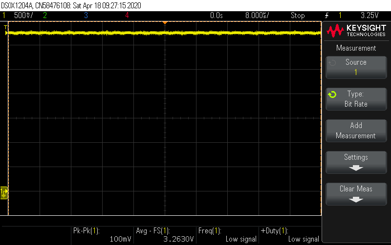
Image 1: VOUT @ VIN = 8,4V

Image 2: SW @ VIN = 8,4V
Raising VIN seems to increase ripple on VOUT and SW begins to look wrong.
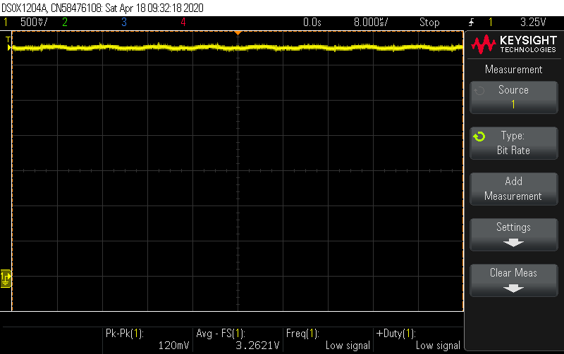
Image 3: VOUT @ VIN = 8,7V

Image 4: SW @ VIN = 8,7V
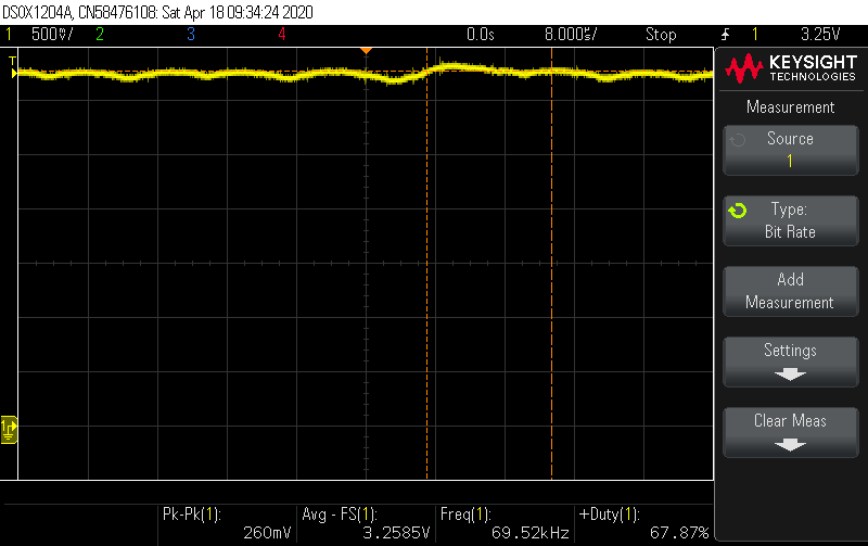
Image 5: VOUT @ VIN = 11,7V
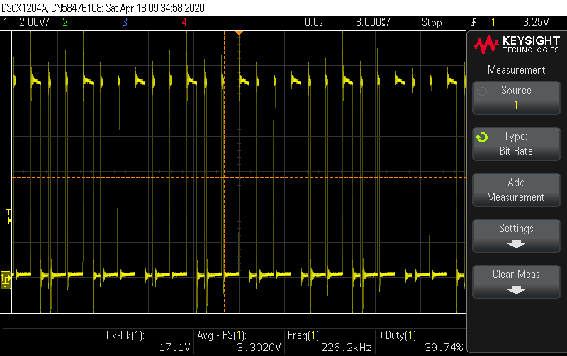
Image 6: SW @ VIN = 11,7V
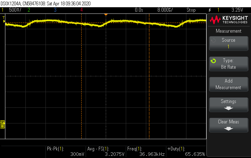
Image 7: VOUT @ VIN = 15,7V

Image 8: SW @ VIN = 15,7V

Image 9: VOUT @ VIN = 20,2V

Image 10: SW @ VIN = 20,2V
As you can see ripple increases significantly.
This proceeds until VIN = 20,4V. Around 20,4V a very high audible noise occurs. Above this, the signals look nice again, and power consumption drops to ~50% just after the signals look nice again.
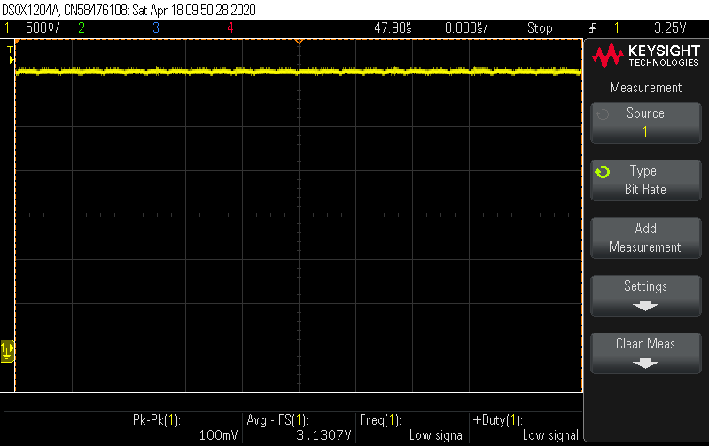
Image 11: VOUT @ VIN = 20,5V

Image 12: SW @ VIN = 20,5V
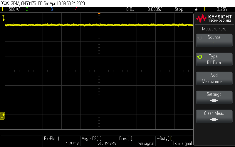
Image 13: VOUT @ VIN = 23,6V

Image 14: SW @ VIN = 23,6V
Some observations:
1. VOUT drop when increasing VIN. VOUT = 3,24V @ VIN = 4,7V /\ VOUT = 3,08V @ VIN = 23,6V
2. During the middle phase (8,6V - 20,4V) current consumption stays the same indicating poor performance from the regulator. In the outer phases were everything seems good we are pulling ~400mW.
4,7V VIN = 0,08mA
8,7V VIN = 0,06mA
11,7V VIN = 0,06mA
15,7V VIN = 0,06mA
18,7V VIN = 0,06mA
20,1V VIN = 0,06mA
20,7V VIN = 0,02mA
This is mounted on a PCB from a PCB manufacturer.
I have double checked all solderings and on a second board manually double soldered all solderings.
This issue persists across 3 different prototypes.
See below for schematic and PCB of circuit.
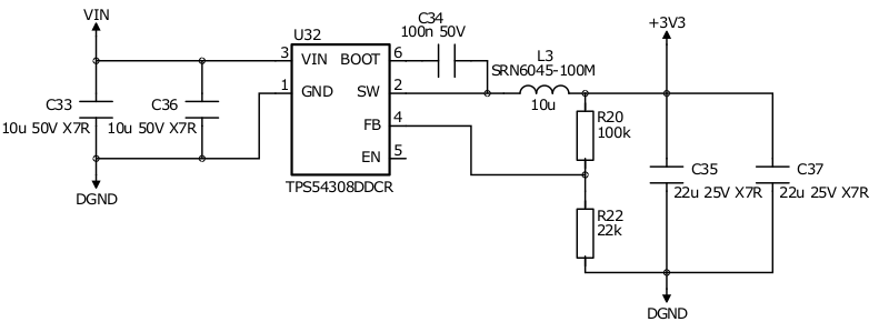
Image 15: Schematic of circuit.

Image 16: PCB layout of circuit.
I'd appreciate some assistance ASAP as this product is pending my approval for he manufacturer to continue.
Regards Mathias
